
* Product structure: Silicon monolithic integrated circuit. ** This product is not designed to protect against radioactive rays.
Copyright: 2017 ROHM Co., Ltd. All rights reserved.
http://www.rohm.com/
1/127
TSZ22111-14-001
TSZ02201-0B4B0A700040-1-2
18. Jul. 2017, Rev.001
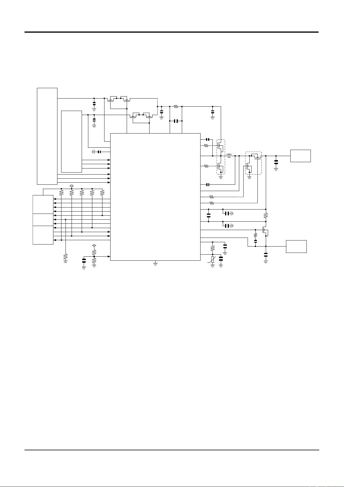
1 to 4-Cell Li-Ion Battery Manager
For Application Processors
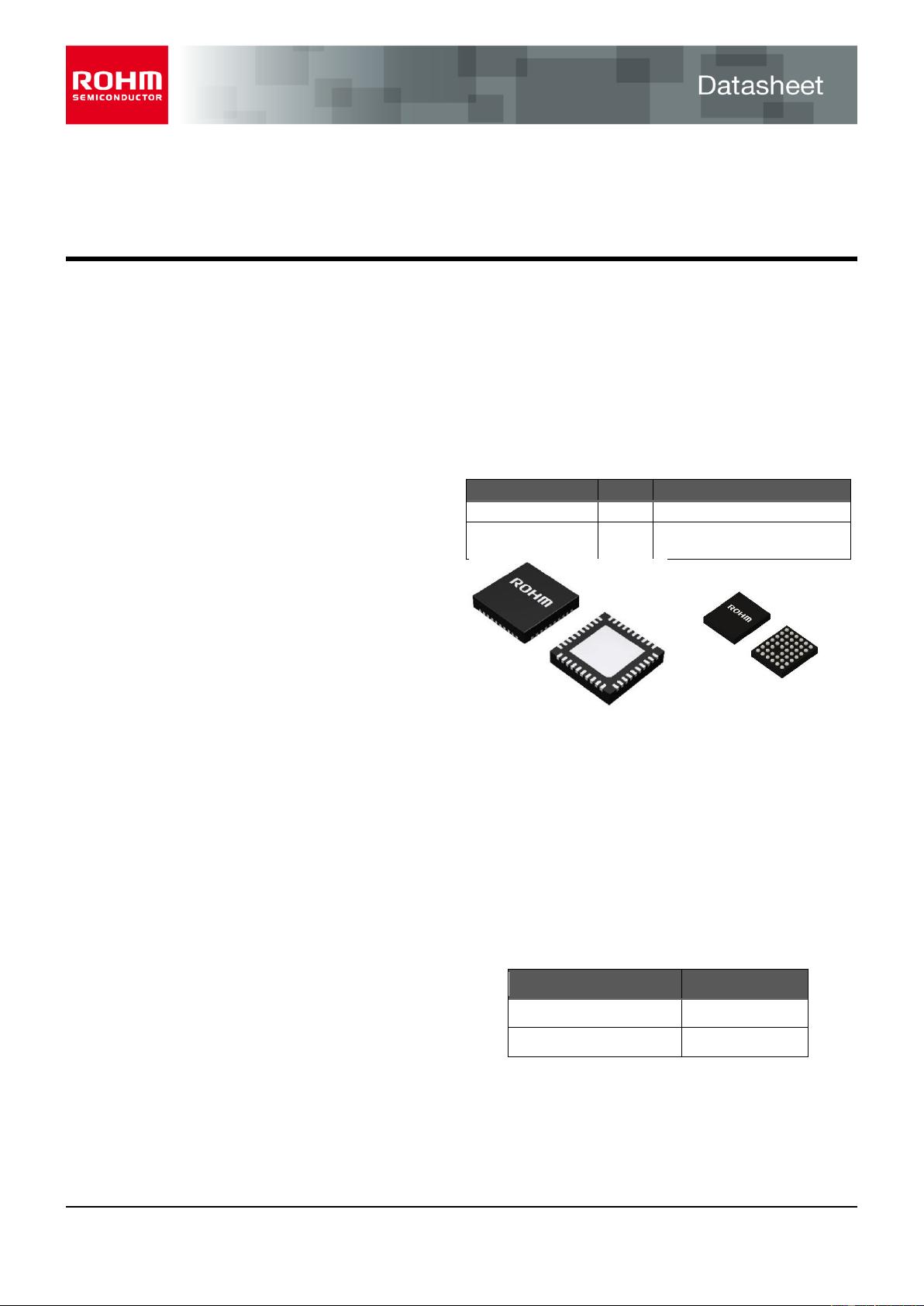
BD99954MWV, BD99954GW
General Description
BD99954 is a Battery Management LSI for 1-4 cell
Lithium-Ion secondary battery, and available in a 40pin
0.40 mm pitch 5.0 mm x 5.0 mm QFN package and small
41-ball 0.4mm pitch 2.6mm x 3.0mm Wafer-Level CSP
package which is designed to meet high degree demands
for space-constraint equipment such as Low profile
Notebook PC, Tablets and other applications.
BD99954 provides a Dual-source Battery Charger, two
port BC1.2 detection and a Battery Monitor with several
alarm(INT#, PROCHOT#) outputs
Features
Dual-source Battery Charger
High efficiency Step-Up/Down switching charger for
1-4 cell Li-Ion/Li-poly battery
Two separate input sources for USB-VBUS and DC
adapter.
Two port BC1.2 detectors.
JEITA compliant charging profile
Programmable parameters for Preconditioning, Pre-
charge current, and Fast-charge current
Programmable charging voltage
Programmable charge current
Programmable Switching Frequency: 600kHz to
1.2MHz
Support USB BCS 1.2, ACA, ID pin, OTG
USB-VBUS Over Voltage Protection
Over Voltage Battery Protection
Battery Short Circuit Detection
Power Path Management with charge pump gate
driver
Flexibility power path control
Reverse Buck/Boost Option for USB/USB-PD
Bias voltage output for the external thermistor
PMON output
PROCHOT# output
Support Inhibit / Autonomous Charging
Battery Learn Function
Input Operating Range: 3.8V to 25V
Voltage Measurement for Thermistor.
Bias voltage output for the external thermistor.
SMBus Interface (Clock up friendly I2C) for Host
communication
Embedded OTPROM for initial settings
Packages
Pitch
W
x
D
x
H
UQFN040V5050
0.4mm
5.0mm
x
5.0mm
x
1.0mm
UCSP55M3C
6 x 7balls
0.4mm
2.6mm
x
3.0mm
x
0.62mm
UQFN040V5050
UCSP55M3C
Applications
Ultrabook
Notebook PC
Ultra-mobile PC
Tablet PC
Structure
Silicon Monolithic Integrated Circuit
Line up matrix
Parts No.
Package
BD99954MWV
UQFN040V5050
BD99954GW
UCSP55M3C

剩余129页未读,继续阅读
资源评论


源码注释器
- 粉丝: 18
- 资源: 37


最新资源
- python图片转字符
- 【java毕业设计】客户关系管理系统源码(ssm+mysql+说明文档).zip
- 【java毕业设计】酒店客房预定管理系统源码(ssm+mysql+说明文档+LW).zip
- 【java毕业设计】教师业务数据统计与分析系统源码(ssm+mysql+说明文档).zip
- cp105b,cp205,cp205w,cp215,cp215w寿命重置工具,解决091-402
- 【java毕业设计】健身房管理系统源码(ssm+mysql+说明文档).zip
- py test for self
- ui-auto test for self
- 【java毕业设计】基于推荐算法的图书购物网站源码(ssm+mysql+说明文档+LW).zip
- appium test for self
资源上传下载、课程学习等过程中有任何疑问或建议,欢迎提出宝贵意见哦~我们会及时处理!
点击此处反馈


