Features
Copyright © 2008 Marvell Doc. No. MV-S104987-U0 Rev. F
December 2, 2008, Preliminary Document Classification: Proprietary Information Page 5
FEATURES
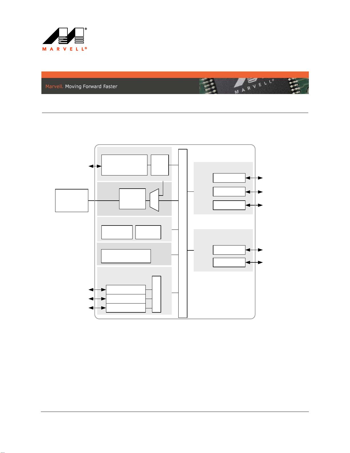
88F6190 – Incorporates a single GbE port and a single
SATA port. CPU speed is up to 600 MHz.
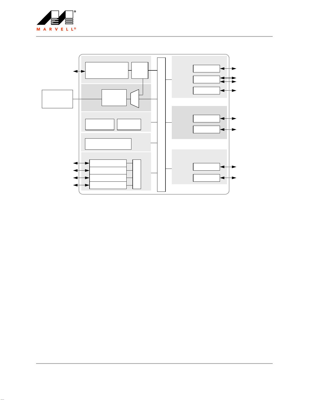
88F6192 – Incorporates two GbE ports and two SATA
ports. CPU speed is up to 800 MHz. It also supports a
Sony/Philips Digital Interconnect Format / Integrated
Interchip Sound (S/PDIF / I
2
S) Audio interface, a TDM
SLIC/SLAC Codec interface, and an MPEG Transport
Stream (TS)
interface.
The 88F6190 and 88F6192 controllers include:
• High-performance CPU core, running at up to
600 MHz in the 88F6190 or 800 MHz in the
88F6192, with integrated, four-way, set-associative
L1 16-KB I-cache/16-KB D-cache and unified,
256-KB, four-way, set-associative L2 cache
• High-bandwidth dual-port DDR2 memory interface
(16-bit DDR2 SDRAM @ up to 400 MHz data rate)
• PCI Express (x1) port with integrated PHY
• Gigabit Ethernet (10/100/1000 Mbps) MAC(s)
• USB 2.0 port with integrated PHY
•
SATA 2.0 port(s) with integrated 3 Gbps SATA II PHY
• Security Cryptographic engine
• S/PDIF / I
2
S Audio in/out interface (88F6192 only)
• SD/SDIO/MMC interface
• TDM SLIC/SLAC Codec interface (88F6192 only)
• Two XOR engines, each containing two XOR/DMA
channels (a total of four XOR/DMA channels)
• MPEG Transport Stream (TS) interface
(88F6192 only)
• SPI port with SPI flash boot support
• 8-bit NAND flash interface with boot support
• Two 16550 compatible UART interfaces
• TWSI port
• 36 multi-purpose pins
• Internal Real Time Clock (RTC)
• Interrupt controller
• Timers
• 128-bit eFuse (one-time programmable memory)
Sheeva
™
CPU core
• 88F6190 – Up to 600 MHz
• 88F6192 – Up to 800 MHz
• 32-bit and 16-bit RISC architecture
• Compliant with v5TE architecture, as published in
the ARM Architect Reference Manual, Second
Edition
• Includes MMU to support virtual memory features
• 256-KB, four-way, set-associative L2 unified cache
• 16-KB, four-way, set-associative I-cache
• 16-KB, four-way, set-associative D-cache
• 64-bit internal data bus
• Branch Prediction unit
• Supports JTAG/ARM ICE
• Supports both Big and Little Endian modes
DDR2 SDRAM controller
• 16-bit interface
•
Up to 200 MHz clock frequency (400 MHz data rate)
• DDR SDRAM with a clock ratio of 1:N and 2:N
between the DDR SDRAM and the CPU core,
respectively
• SSTL 1.8V I/Os
• Auto calibration of I/Os output impedance
• Supports two DRAM chip selects
• Supports all DDR devices densities up to1 Gb
• Supports up to16 open pages (page per bank)
• Up to 512 MB total address space
•
Supports on-board DDR designs (no DIMM support)
• Supports 2T mode, to enable high-frequency
operation under heavy load configuration
• Supports DRAM bank interleaving
• Supports up to a 128-byte burst per single memory
access
PCI Express interface (x1)
• PCI Express Base 1.1 compatible
• Integrated low-power SERDES PHY, based on
proven Marvell
®
SERDES technology
• Serves as a Root Complex or an Endpoint port
• x1 link width
• 2.5 Gbps data rate
• Lane polarity reversal support
• Maximum payload size of 128 bytes
• Single Virtual Channel (VC-0)
• Replay buffer support
• Extended PCI Express configuration space
• Advanced Error Reporting (AER) support
• Power management: L0s and software L1 support
• Interrupt emulation message support
• Error message support
PCI Express master specific features
• Single outstanding read transaction
• Maximum read request of up to 128 bytes
• Maximum write request of up to 128 bytes
• Up to four outstanding read transactions in
Endpoint mode
PCI Express target specific features
• Supports up to eight read request transactions
• Maximum read request size of 4 KB
• Maximum write request of 128 bytes


 我的内容管理
展开
 我的资源
快来上传第一个资源
 我的收益 登录查看自己的收益
 我的积分
登录查看自己的积分
 我的C币
登录后查看C币余额
 我的收藏
我的收藏  我的下载
我的下载  下载帮助
下载帮助 
 前往需求广场,查看用户热搜

 信息提交成功