Aptina reserves the right to change products or specifications without notice.
AR0130 Registers - Rev. C Pub. 2/14 EN
2 ©2011 Aptina Imaging Corporation. All rights reserved.
AR0130: Register Reference
Introduction
Aptina Confidential and Proprietary
Introduction
This register reference is provided for engineers who are designing cameras that use the
AR0130.
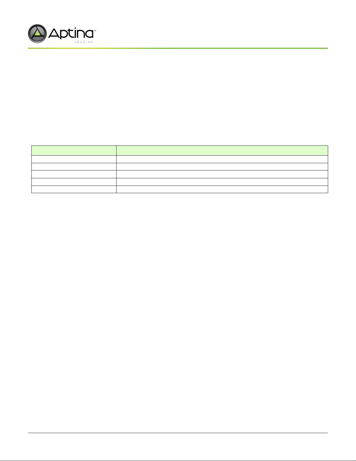
Register Address Space
The AR0130 provide a 16-bit register address space accessed through a serial interface.
Each register location is 8 or 16 bits in size.
The address space is divided into the five major regions shown in Table 1.
Register Notation
The underlying mechanism for reading and writing registers provides byte write capa-
bility. However, it is convenient to consider some registers as multiple adjacent bytes.
The AR0130 use 8-bit, 16-bit, and 32-bit registers, all implemented as 1 or more bytes at
naturally aligned, contiguous locations in the address space.
In this document, registers are described either by address or by name. When registers
are described by address, the size of the registers is explicit. For example, R0x3024 is an
8-bit register at address 0x3024, and R0x3000
–1 is a 16-bit register at address 0x3000–
0x3001. When registers are described by name, the size of the register is implicit. It is
necessary to refer to the register table to determine that model_id is a 16-bit register.
Register Aliases
A consequence of the internal architecture of the AR0130 is that some registers are
decoded at multiple addresses. Some registers in “configuration space” are also decoded
in “manufacturer-specific space.” To provide unique names for all registers, the name of
the register within manufacturer-specific register space has a trailing underscore. For
example, R0x0000
–1 is model_id, and R0x3000–1 is model_id_. The effect of reading or
writing a register through any of its aliases is identical.
Bit Fields
Some registers provide control of several different pieces of related functionality, and
this makes it necessary to refer to bit fields within registers. As an example of the nota-
tion used for this, the least significant 4 bits of the model_id register are referred to as
model_id[3:0] or R0x0000
–1[3:0].
Table 1: Address Space Regions
Address Range Description
0x0000–0x0FFF Reserved
0x1000–0x1FFF Reserved
0x2000–0x2FFF Reserved
0x3000–0x3FFF Manufacturer-specific registers (read-only and read-write dynamic registers)
0x4000–0xFFFF Reserved


 newmsg_sdr2019-11-05资料可以,就是太贵了,C版本的,我刚刚上传了D版本的,更新,只要5个积分。


