
ADC0831/ADC0832/ADC0834/ADC0838
8-Bit Serial I/O A/D Converters with Multiplexer Options
General Description
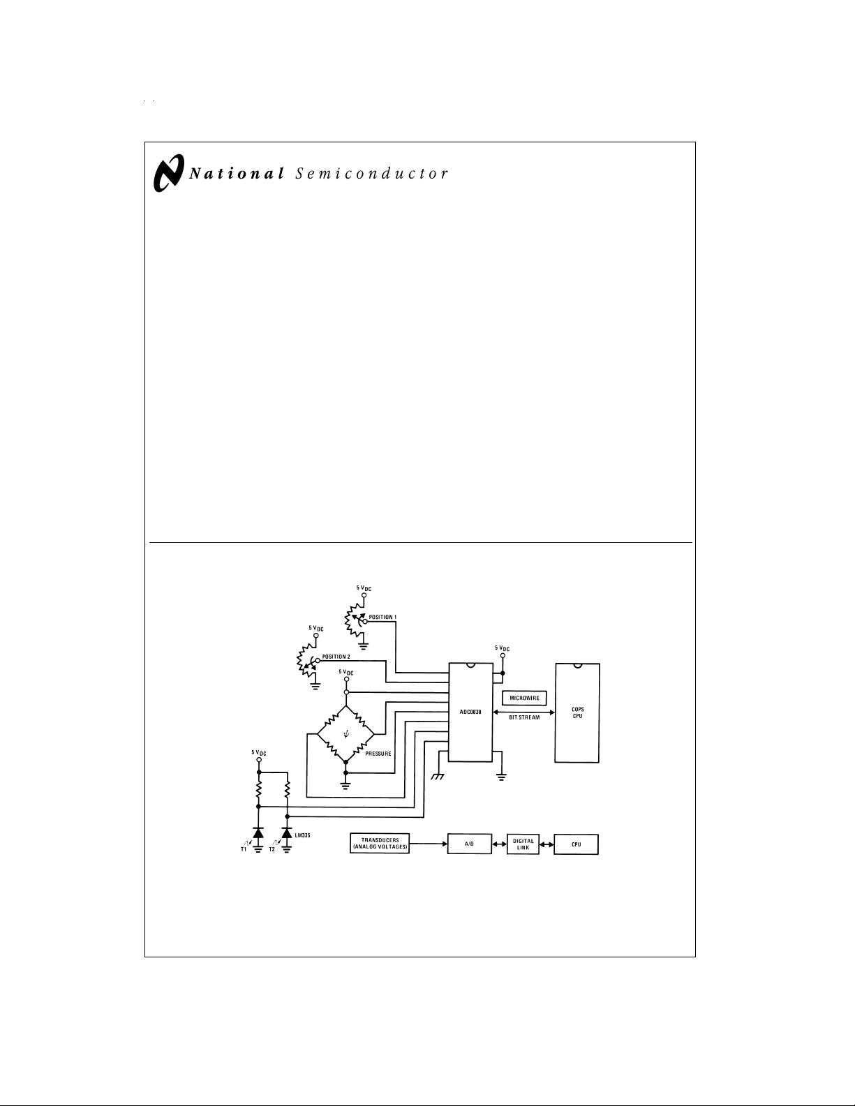
The ADC0831 series are 8-bit successive approximation A/D
converters with a serial I/O and configurable input multiplex-
ers with up to 8 channels. The serial I/O is configured to
comply with the NSC MICROWIRE
™
serial data exchange
standard for easy interface to the COPS
™
family of proces-
sors, and can interface with standard shift registers or µPs.
The 2-, 4- or 8-channel multiplexers are software configured
for single-ended or differential inputs as well as channel as-
signment.
The differential analog voltage input allows increasing the
common-mode rejection and offsetting the analog zero input
voltage value. In addition, the voltage reference input can be
adjusted to allow encoding any smaller analog voltage span
to the full 8 bits of resolution.
Features
n NSC MICROWIRE compatible — direct interface to
COPS family processors
n Easy interface to all microprocessors, or operates
“stand-alone”
n Operates ratiometrically or with 5 V
DC
voltage
reference
n No zero or full-scale adjust required
n 2-, 4- or 8-channel multiplexer options with address logic
n Shunt regulator allows operation with high voltage
supplies
n 0V to 5V input range with single 5V power supply
n Remote operation with serial digital data link
n TTL/MOS input/output compatible
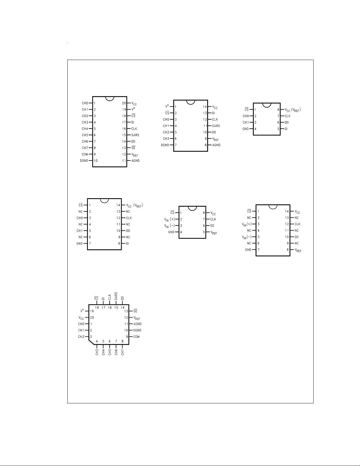
n 0.3" standard width, 8-, 14- or 20-pin DIP package
n 20 Pin Molded Chip Carrier Package (ADC0838 only)
n Surface-Mount Package
Key Specifications
n Resolution 8 Bits
n Total Unadjusted Error
±
1
⁄
2
LSB and
±
1 LSB
n Single Supply 5 V
DC
n Low Power 15 mW
n Conversion Time 32 µs
Typical Application
TRI-STATE
®
is a registered trademark of National Semiconductor Corporation.
COPS
™
and MICROWIRE
™
are trademarks of National Semiconductor Corporation.
DS005583-1
August 1999
ADC0831/ADC0832/ADC0834/ADC0838 8-Bit Serial I/O A/D Converters with Multiplexer Options
© 1999 National Semiconductor Corporation DS005583 www.national.com

剩余31页未读,继续阅读


评论0
最新资源