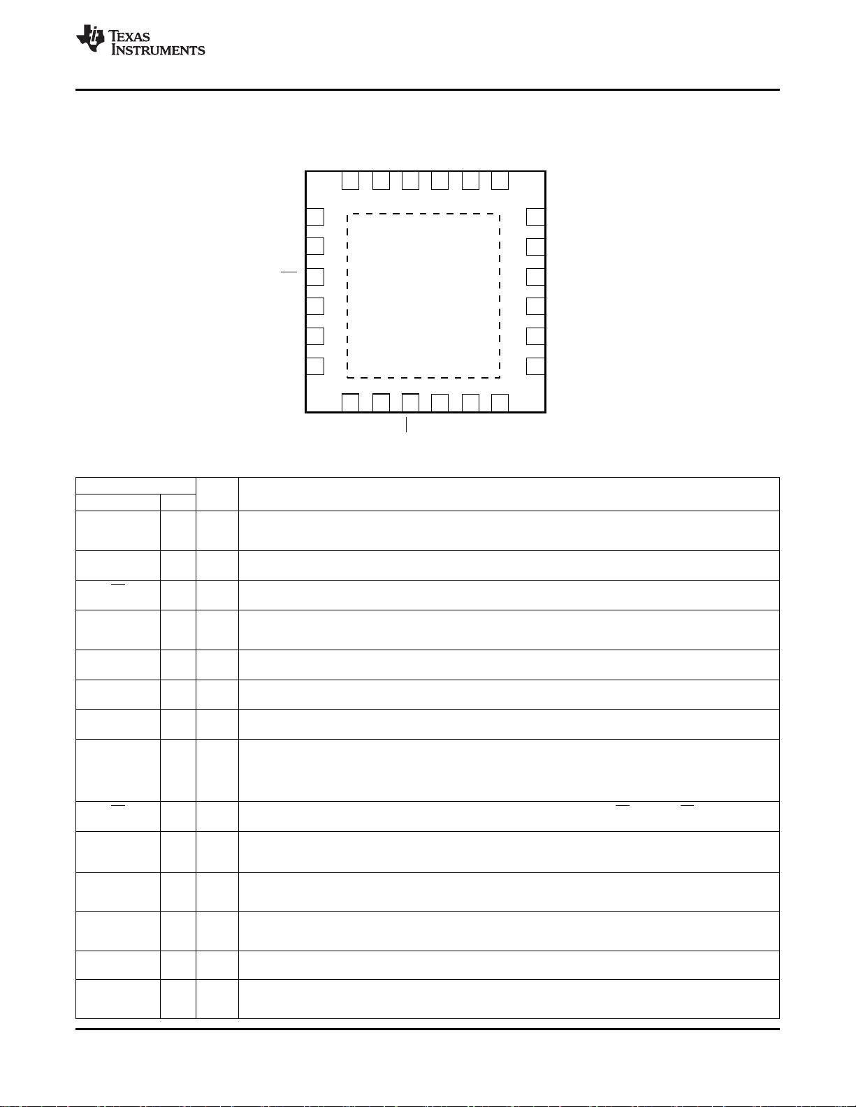
STAT
SCL
SDA
VBUS
PMID
REGN
PGND
PGND
SYS
SYS
OTG
INT
4
5
6
7 8 9
15
16
17
18
22
23
24
1
2
3
BAT
BAT
13
14
BTST
SW
SW
1920
21
10
11 12
VBUS
PSEL
PG
ILIM
TS1
TS2
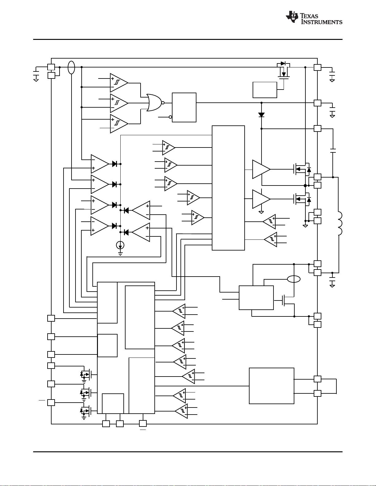
bq24196
CE
bq24196
www.ti.com.cn
ZHCSAD5 –OCTOBER 2012
PINOUTS
PIN FUNCTIONS
PIN
TYPE DESCRIPTION
NAME NO.
VBUS 1,24 P Charger Input Voltage. The internal n-channel reverse block MOSFET (RBFET) is connected between VBUS and PMID
with VBUS on source. Place a 1µF ceramic capacitor from VBUS to PGND and place it as close as possible to IC. (Refer
to Application Information Section for details)
PSEL – I Power source selection input. High indicates a USB host source and Low indicates an adapter source.
Digital
PG – O Open drain active low power good indicator. Connect to the pull up rail via 10kohm resistor. LOW indicates a good input
source if the input voltage is between UVLO and ACOV, above SLEEP mode threshold, and current limit is above 30mA.
Digital
STAT 4 O Open drain charge status output to indicate various charger operation. Connect to the pull up rail via 10kohm. LOW
indicates charge in progress. HIGH indicates charge complete or charge disabled. When any fault condition occurs, STAT
Digital
pin blinks at 1Hz.
SCL 5 I
I
2
C Interface clock. Connect SCL to the logic rail through a 10kΩ resistor.
Digital
SDA 6 I/O
I
2
C Interface data. Connect SDA to the logic rail through a 10kΩ resistor.
Digital
INT 7 O Open-drain Interrupt Output. Connect the INT to a logic rail via 10kΩ resistor. The INT pin sends active low, 256us pulse
to host to report charger device status and fault.
Digital
OTG 8 I USB current limit selection pin during buck mode, and active high enable pin during boost mode.
Digital
In buck mode with USB host (PSEL=High), when OTG = High, IIN limit = 500mA and when OTG = Low, IIN limit =
100mA.
The boost mode is activated when the REG01[5:4]=10 and OTG pin is High.
CE 9 I Active low Charge Enable pin. Battery charging is enabled when REG01[5:4]=01 and CE pin = Low. CE pin must be
pulled high or low.
Digital
ILIM 10 I ILIM pin sets the maximum input current limit by regulating the ILIM voltage at 1V. A resistor is connected from ILIM pin to
ground to set the maximum limit as I
INMAX
= (1V/R
ILIM
) × 530. The actual input current limit is the lower one set by ILIM
Analog
and by I
2
C REG00[2:0]. The minimum input current programmed on ILIM pin is 500mA.
TS1 11 I Temperature qualification voltage input #1. Connect a negative temperature coefficient thermistor. Program temperature
window with a resistor divider from REGN to TS1 to GND. Charge suspends when either TS pin is out of range.
Analog
Recommend 103AT-2 thermistor.
TS2 12 I Temperature qualification voltage input #2. Connect a negative temperature coefficient thermistor. Program temperature
window with a resistor divider from REGN to TS2 to GND. Charge suspends when either TS pin is out of range.
Analog
Recommend 103AT-2 thermistor. TS1 and TS2 pin can be connected together for single thermistor application.
BAT 13,14 P Battery connection point to the positive terminal of the battery pack. The internal BATFET is connected between BAT and
SYS. Connect a 10uF closely to the BAT pin.
SYS 15,16 P System connection point. The internal BATFET is connected between BAT and SYS. When the battery falls below the
minimum system voltage, switch-mode converter keeps SYS above the minimum system voltage. (Refer to Application
Information Section for inductor and capacitor selection)
Copyright © 2012, Texas Instruments Incorporated 5


 我的内容管理
展开
 我的资源
快来上传第一个资源
 我的收益 登录查看自己的收益
 我的积分
登录查看自己的积分
 我的C币
登录后查看C币余额
 我的收藏
我的收藏  我的下载
我的下载  下载帮助
下载帮助 
 前往需求广场,查看用户热搜

 信息提交成功