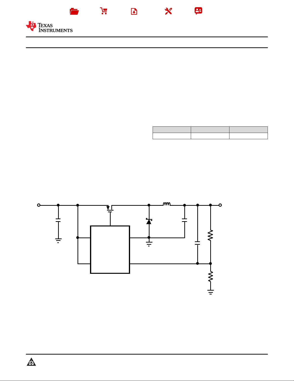
没有合适的资源?快使用搜索试试~ 我知道了~
DCDC芯片 lm3475规格书
资源推荐
资源详情
资源评论
V
OUT
= 2.5V/2A
C
IN
C
OUT
R
FB1
R
FB2
L1
D1
Q1
10 PF
100 PF
10 PH
1k
2.15k
Si2343
LM3475
V
IN
EN
GND
PGATE
FB
1
2
3
4
5
C
FF
1 nF
V
IN
= 5V
Product
Folder
Sample &
Buy
Technical
Documents
Tools &
Software
Support &
Community
LM3475
SNVS239C –OCTOBER 2004–REVISED OCTOBER 2015
LM3475 Hysteretic PFET Buck Controller
1 Features 3 Description
The LM3475 is a hysteretic P-FET buck controller
1
• Easy-to-Use Control Methodology
designed to support a wide range of high efficiency
• 0.8 V to V
IN
Adjustable Output Range
applications in a very small SOT-23-5 package. The
• High Efficiency (90% Typical)
hysteretic control scheme has several advantages,
including simple system design with no external
• ±0.9% (±1.5% Over Temperature) Feedback
compensation, stable operation with a wide range of
Voltage
components, and extremely fast transient response.
• 100% Duty Cycle Capable
Hysteretic control also provides high efficiency
• Maximum Operating Frequency up to 2 MHz
operation, even at light loads. The PFET architecture
allows for low component count as well as 100% duty
• Internal Soft-Start
cycle and ultra-low dropout operation.
• Enable Pin
Device Information
(1)
2 Applications
PART NUMBER PACKAGE BODY SIZE (NOM)
• TFT Monitor
LM3475 SOT-23 (5) 1.60 mm × 2.90 mm
• Auto PC
(1) For all available packages, see the orderable addendum at
• Vehicle Security the end of the data sheet.
• Navigation Systems
• Notebook Standby Supply
• Battery Powered Portable Applications
• Distributed Power Systems
Typical Application
1
An IMPORTANT NOTICE at the end of this data sheet addresses availability, warranty, changes, use in safety-critical applications,
intellectual property matters and other important disclaimers. PRODUCTION DATA.
LM3475
SNVS239C –OCTOBER 2004–REVISED OCTOBER 2015
www.ti.com
Table of Contents
7.4 Device Functional Modes........................................ 10
1 Features.................................................................. 1
8 Application and Implementation ........................ 11
2 Applications ........................................................... 1
8.1 Application Information............................................ 11
3 Description ............................................................. 1
8.2 Typical Application ................................................. 11
4 Revision History..................................................... 2
9 Power Supply Recommendations...................... 16
5 Pin Configuration and Functions......................... 3
10 Layout................................................................... 16
6 Specifications......................................................... 4
10.1 Layout Guidelines ................................................. 16
6.1 Absolute Maximum Ratings ...................................... 4
10.2 Layout Example .................................................... 17
6.2 ESD Ratings.............................................................. 4
11 Device and Documentation Support ................. 18
6.3 Recommended Operating Ratings ........................... 4
11.1 Device Support...................................................... 18
6.4 Thermal Information.................................................. 4
11.2 Community Resources.......................................... 18
6.5 Electrical Characteristics........................................... 5
11.3 Trademarks........................................................... 18
6.6 Typical Characteristics.............................................. 6
11.4 Electrostatic Discharge Caution............................ 18
7 Detailed Description.............................................. 8
11.5 Glossary................................................................ 18
7.1 Overview ................................................................... 8
12 Mechanical, Packaging, and Orderable
7.2 Functional Block Diagram ......................................... 8
Information ........................................................... 18
7.3 Feature Description................................................... 8
4 Revision History
NOTE: Page numbers for previous revisions may differ from page numbers in the current version.
Changes from Revision B (March 2013) to Revision C Page
• Added ESD Ratings table, Feature Description section, Device Functional Modes, Application and Implementation
section, Power Supply Recommendations section, Layout section, Device and Documentation Support section, and
Mechanical, Packaging, and Orderable Information section. ................................................................................................. 1
Changes from Revision A (March 2013) to Revision B Page
• Changed layout of National Data Sheet to TI format. ........................................................................................................... 1
2 Submit Documentation Feedback Copyright © 2004–2015, Texas Instruments Incorporated
Product Folder Links: LM3475
PGATE
GND
FB
VIN
1
2
3
4
5
EN
LM3475
www.ti.com
SNVS239C –OCTOBER 2004–REVISED OCTOBER 2015
5 Pin Configuration and Functions
DBV Package
5-Pin SOT-23
Top View
Pin Functions
PIN
I/O DESCRIPTION
NAME NO.
FB 1 I Feedback input. Connect to a resistor divider between the output and GND.
GND 2 G Ground.
Enable. Pull this pin above 1.5 V (typical) for normal operation. When EN is low, the device
EN 3 O
enters shutdown mode.
VIN 4 P Power supply input.
PGATE 5 O Gate drive output for the external PFET.
Copyright © 2004–2015, Texas Instruments Incorporated Submit Documentation Feedback 3
Product Folder Links: LM3475
LM3475
SNVS239C –OCTOBER 2004–REVISED OCTOBER 2015
www.ti.com
6 Specifications
6.1 Absolute Maximum Ratings
See
(1)(2)
MIN MAX UNIT
V
IN
−0.3 16 V
PGATE −0.3 16 V
FB −0.3 5 V
EN −0.3 16 V
Power dissipation
(3)
440 mW
Vapor phase (60 s) 215
Lead temperature °C
Infrared (15 s) 220
T
stg
Storage temperature −65 1150 °C
(1) Stresses beyond those listed under Absolute Maximum Ratings may cause permanent damage to the device. These are stress ratings
only, which do not imply functional operation of the device at these or any other conditions beyond those indicated under Recommended
Operating Conditions. Exposure to absolute-maximum-rated conditions for extended periods may affect device reliability.
(2) If Military/Aerospace specified devices are required, please contact the Texas Instruments Sales Office/ Distributors for availability and
specifications.
(3) The maximum allowable power dissipation is a function of the maximum junction temperature, T
J_MAX
, the junction-to-ambient thermal
resistance, θ
JA
and the ambient temperature, T
A
. The maximum allowable power dissipation at any ambient temperature is calculated
using: P
D_MAX
= (T
J_MAX
- T
A
)/θ
JA
. The maximum power dissipation of 0.44 W is determined using T
A
= 25°C, θ
JA
= 225°C/W, and
T
J_MAX
= 125°C.
6.2 ESD Ratings
over operating free-air temperature range (unless otherwise noted)
VALUE UNIT
V
(ESD)
Electrostatic discharge Human-body model (HBM), per ANSI/ESDA/JEDEC JS-001
(1)
2500 V
(1) JEDEC document JEP155 states that 500-V HBM allows safe manufacturing with a standard ESD control process.
6.3 Recommended Operating Ratings
MIN NOM MAX UNIT
Supply voltage 2.7 10 V
T
J
Operating junction temperature -40 125 °C
6.4 Thermal Information
LM3475
THERMAL METRIC
(1)
DBV (SOT-23) UNIT
5 PINS
R
θJA
Junction-to-ambient thermal resistance 164.2 °C/W
R
θJC(top)
Junction-to-case (top) thermal resistance 115.3 °C/W
R
θJB
Junction-to-board thermal resistance 27.0 °C/W
ψ
JT
Junction-to-top characterization parameter 12.8 °C/W
ψ
JB
Junction-to-board characterization parameter 26.5 °C/W
R
θJC(bot)
Junction-to-case (bottom) thermal resistance N/A °C/W
(1) For more information about traditional and new thermal metrics, see the Semiconductor and IC Package Thermal Metrics application
report, SPRA953.
4 Submit Documentation Feedback Copyright © 2004–2015, Texas Instruments Incorporated
Product Folder Links: LM3475
LM3475
www.ti.com
SNVS239C –OCTOBER 2004–REVISED OCTOBER 2015
6.5 Electrical Characteristics
Typical limits are for T
J
= 25°C, unless otherwise specified, V
IN
= EN = 5.0 V. Maximum and minimum specification limits are
specified by design, test, or statistical analysis.
PARAMETER TEST CONDITIONS MIN TYP MAX UNIT
I
Q
Quiescent current EN = V
IN
(PGATE T
J
= 25°C 260
Open)
T
J
= −40°C to +125°C 170 320
µA
EN = 0V T
J
= 25°C 7
T
J
= −40°C to +125°C 4 10
V
FB
T
J
= 25°C 0.8
Feedback voltage V
T
J
= −40°C to +125°C 0.788 0.812
%ΔV
FB
/ΔV
IN
Feedback voltage line
2.7 V < V
IN
< 10 V 0.01 %/V
regulation
V
HYST
Comparator hysteresis 2.7 V < V
IN
< 10 V T
J
= 25°C 21 28
mV
−40°C to +125°C 21 32
I
FB
FB bias current T
J
= 25°C 50 nA
−40°C to +125°C 600
Enable threshold Increasing T
J
= 25°C 1.5
V
voltage
Vth
EN
−40°C to +125°C 1.2 1.8
Hysteresis 365 mV
I
EN
Enable leakage current T
J
= 25°C 0.025
EN = 10 V µA
−40°C to +125°C 1
Source
2.8
I
SOURCE
= 100 mA
R
PGATE
Driver resistance Ω
Sink
1.8
I
Sink
= 100 mA
Source
V
PGATE
= 3.5 V 0.475
C
PGATE
= 1 nF
I
PGATE
Driver output current A
Sink
V
PGATE
= 3.5 V 1.0
C
PGATE
= 1 nF
T
SS
Soft-start time 2.7 V < V
IN
< 10 V (EN Rising) 4 ms
T
ONMIN
Minimum on-time PGATE Open 180 ns
V
UVD
Undervoltage detection Measured at the FB T
J
= 25°C 0.56
V
Pin
−40°C to +125°C 0.487 0.613
Copyright © 2004–2015, Texas Instruments Incorporated Submit Documentation Feedback 5
Product Folder Links: LM3475
剩余24页未读,继续阅读
资源评论
yhw1984
- 粉丝: 0
- 资源: 1
上传资源 快速赚钱
- 我的内容管理 展开
- 我的资源 快来上传第一个资源
- 我的收益 登录查看自己的收益
- 我的积分 登录查看自己的积分
- 我的C币 登录后查看C币余额
- 我的收藏
- 我的下载
- 下载帮助
最新资源
- rdf0412-kcu116-pcie-c-2019-1.zip(XILINX KCU116 源码)
- 基于C#语言的winform界面火车票订票系统(源码+实验报告)
- 【华为OD部分真题及讲解】华为OD部分真题及讲解
- 基于Python+Django的京东商品比价系统源码+全部资料(毕业设计).zip
- G460 G560 Z460 Z560的最新BIOS 2.18版(无白名单)
- MetaJUI v0.4
- 基于Python+Django的京东商品比价系统源码+全部资料(毕业设计).zip
- linux常用命令大全
- 立体相机标定-使用OpenCV+Cpp对立体相机进行标定-calibration-附项目源码+流程教程-优质项目实战.zip
- 基于SpringBoot+Mysql开发的酒店管理系统
资源上传下载、课程学习等过程中有任何疑问或建议,欢迎提出宝贵意见哦~我们会及时处理!
点击此处反馈
安全验证
文档复制为VIP权益,开通VIP直接复制
信息提交成功