
© Semiconductor Components Industries, LLC, 2009
September, 2009 − Rev. 0
1 Publication Order Number:
NTMS4937N/D
NTMS4937N
Power MOSFET
30 V, 13.6 A, N−Channel, SO−8
Features
• Low R
DS(on)
to Minimize Conduction Losses
• Low Capacitance to Minimize Driver Losses
• Optimized Gate Charge to Minimize Switching Losses
• These Devices are Pb−Free, Halogen Free/BFR Free and are RoHS
Compliant
Applications
• DC−DC Converters
• Points of Loads
• Power Load Switch
• Motor Controls
MAXIMUM RATINGS (T
J
= 25°C unless otherwise stated)
Parameter
Symbol Value Unit
Drain−to−Source Voltage V
DSS
30 V
Gate−to−Source Voltage V
GS
±20 V
Continuous Drain
Current R
q
JA
(Note 1)
Steady
State
T
A
= 25°C
I
D
11.2
A
T
A
= 70°C 9.0
Power Dissipation R
q
JA
(Note 1)
Steady
State
T
A
= 25°C P
D
1.36 W
Continuous Drain
Current R
q
JA
(Note 2)
Steady
State
T
A
= 25°C
I
D
8.6
A
T
A
= 70°C 6.9
Power Dissipation R
q
JA
(Note 2)
T
A
= 25°C P
D
0.81 W
Continuous Drain
Current R
q
JA
, t v 10 s
(Note 1)
Steady
State
T
A
= 25°C
I
D
13.6
A
T
A
= 70°C 11
Power Dissipation
R
q
JA
, t v 10 s(Note 1)
Steady
State
T
A
= 25°C P
D
2.0 W
Pulsed Drain Current
T
A
= 25°C, t
p
= 10 ms
I
DM
112 A
Operating Junction and Storage Temperature T
J
,
T
stg
−55 to
150
°C
Source Current (Body Diode) I
S
2.1 A
Single Pulse Drain−to−Source Avalanche Energy
(T
J
= 25°C, V
DD
= 30 V, V
GS
= 10 V,
I
L
= 13 A
pk
, L = 1.0 mH, R
G
= 25 W)
E
AS
84.5 mJ
Lead Temperature for Soldering Purposes
(1/8″ from case for 10 s)
T
L
260 °C
THERMAL RESISTANCE MAXIMUM RATINGS
Parameter Symbol Value Unit
Junction−to−Ambient – Steady State (Note 1)
R
q
JA
91.9
°C/W
Junction−to−Ambient – t v 10 s (Note 1)
R
q
JA
61.1
Junction−to−Foot (Drain)
R
q
JF
22.6
Junction−to−Ambient – Steady State (Note 2)
R
q
JA
154.7
Stresses exceeding Maximum Ratings may damage the device. Maximum
Ratings are stress ratings only. Functional operation above the Recommended
Operating Conditions is not implied. Extended exposure to stresses above the
Recommended Operating Conditions may affect device reliability.
1. Surfacemounted on FR4 board using 1 in sq pad size (Cu area = 1.127 in sq
[1 oz] including traces).
2. Surfacemounted on FR4 board using the minimum recommended pad size.
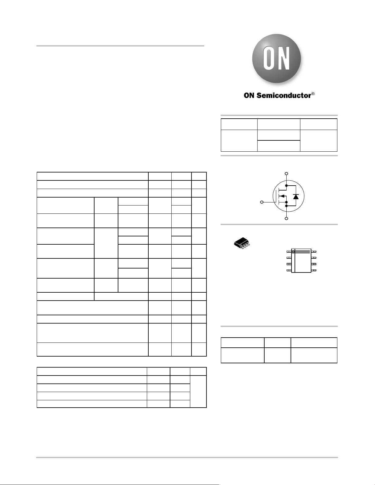
http://onsemi.com
Device Package Shipping
†
ORDERING INFORMATION
V
(BR)DSS
R
DS(ON)
MAX I
D
MAX
30 V
6.5 mW @ 10 V
13.6 A
N−Channel
D
S
G
†For information on tape and reel specifications,
including part orientation and tape sizes, please
refer to our Tape and Reel Packaging Specification
Brochure, BRD8011/D.
SO−8
CASE 751
STYLE 12
MARKING DIAGRAM/
PIN ASSIGNMENT
1
8.7 mW @ 4.5 V
NTMS4937NR2G SO−8
(Pb−Free)
2500/Tape & Reel
4937N
AYWWG
G
4937N = Device Code
A = Assembly Location
Y = Year
WW = Work Week
G = Pb−Free Package
18
Drain
Drain
Drain
Drain
Source
Source
Source
Gate
Top View
(Note: Microdot may be in either location)
资源评论


末哥哥
- 粉丝: 0
- 资源: 1


最新资源
- 2024毕业设计-基于区块链的医疗信息管理系统含论文报告-最新开发.zip
- 2024全球AI创新大赛无人机双光目标检测实战案例(第4名作品).zip
- AGV调度系统的仿真平台(含源码+项目说明+实验结果分析).zip
- AI图像处理工具包-一键抠图、背景切换、旧照片修复、人像漫画化、视频卡通化(Python+OpenCV+Dlib+TensorFlow).zip
- Android恶意软件检测模型-基于机器学习(含源码+项目说明+设计报告).zip
- Ansible部署Kubernetes集群支持多种特定功能StaticPod模式操作手册.zip
- API开放平台-Java开发基于微服务架构的完整解决方案(含源码).zip
- Bilibili数据爬取与分析实战源码+设计报告(Python+Scrapy+LSTM时间序列预测).zip
- ARIMA+Transformer+LSTM心跳时间序列预测模型源码+设计文档(课设新开发项目).zip
- ArcEngine二次开发的专题图自动生成系统(含源码+说明文档+设计报告等全部资料).zip
- BleiData OAG-WholsWho消歧参赛冠军源码.zip
- C++实现腾讯云游长城滑块验证位置计算方法(数学取点法).zip
- C++和Qt开发的五子棋博弈游戏-极大极小搜索+剪枝算法(含设计报告).zip
- CRF与Embedding-Bi-LSTM-CRF医疗数据命名实体识别系统(源码+论文报告).zip
- CCF大数据汽车行业情感分析源码+全部参赛资料.zip
- CCF-BCDI大赛OCR身份证提取冠军源码.zip
资源上传下载、课程学习等过程中有任何疑问或建议,欢迎提出宝贵意见哦~我们会及时处理!
点击此处反馈


