This manual contains text, diagrams and explanations which will guide the reader in the correct installation and
operation of the FX
2N-4AD and should be read and understood before attempting to install or use the unit.
Further information can be found in the FX SERIES PROGRAMMING MANUAL, FX
2N SERIES HARDWARE MANUAL .
• The FX2N-4AD analog special function block has four input channels. The input channels receive analog signals
and convert them into a digital value. This is called an A/D conversion. The FX
2N-4AD has maximum resolution of
12 bits.
• The selection of voltage or current based input/output is by user wiring. Analog ranges of -10 to 10V DC (resolution:
5mV), and/or 4 to 20mA, -20 to 20mA(resolution: 20µA) may be selected.
• Data transfer between the FX2N-4AD and the FX2N main unit is by buffer memory exchange. There are 32 buffer
memories (each of 16 bits) in the FX
2N-4AD.
• The FX2N-4AD occupies 8 points of I/O on the FX2N expansion bus. The 8 points can be allocated from either inputs
or outputs. The FX
2N-4AD draws 30mA from the 5V rail of the FX2N main unit or powered extension unit.
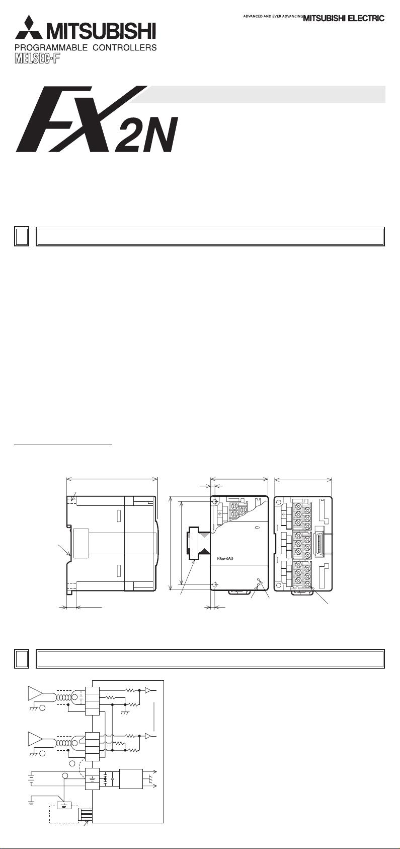
1.1 EXTERNAL DIMENSIONS
Weight : Approx. 0.3 kg (0.66 lbs) Dimensions : mm (inches)
➀ The analog input is received through a twisted pair
shielded cable. This cable should be wired separately
from power lines or any other lines which may induce
electrical noise.
➁ If a voltage ripple occurs during input, or there is
electrically induced noise on the external wiring, connect a
smoothing capacitor of 0.1 to 0.47µF, 25V.
➂ If you are using current input, connect the V+ and I+
terminals to each other.
➃ If there is excessive electrical noise, connect the FG frame
ground terminal with the grounded terminal on the
FX
2N-4AD.
➄ Connect the ground terminal on the FX2N-4AD unit with the
grounded terminal on the main unit. Use class 3
grounding on the main unit, if available.
POWER
A/D
24V
55(2.17)
90(3.54)
4
87(3.43)
FX2N-4AD
55(2.17)
80(3.15)
I+
VI-
V+
I+
VI-
CH4
CH3
CH2
CH1
V+
I+V+
I+
V+
24+
24-
VI-
VI-
FG
FG
FG
9(0.35)
4
Mounting holes
4.5mm(0.18)dia.
DIN rail
Mounting slot
35mm(1.38)
Extension cable
and connector
A/D LED
24V LED
Terminal screws M3(0.12)
CH1
V+
24+
24-
VI-
3.1 Environment specification
Item Specification
Environmental specifications (excluding following) Same as those for the FX
2N main unit
Dielectric withstand voltage 500VAC, 1min (between all terminals and ground)
3.2 Power supply specification
Item Specification
Analog circuits
24V DC ± 10%, 55mA
(external power supply from main unit)
Digital circuits 5V DC, 30mA (internal power supply from main unit)
PC
V+
FG
I+
VI-
Voltage input
-10V to +10V
V+
FG
I+
VI-
Current input
-20mA to +20mA
24-
24+
100KW
100KW
250W
250W
100KW
100KW
CH4
CH1
+15V
AG
-15V
AG
CH4
CH1
1
Shielded
2
3
4
5
1
Shielded
Class 3
Grounding
(100Wor less)
Extension cable
FX
2N-4AD
Analog Input Block
DC24V 55mA
DC/DC
converter
3.3 Performance specification
Analog Inputs
Item
Voltage input Current input
Either voltage or current input can be selected with your choice of input terminal. Up to four
input points can be used at one time.
Analog input range
DC -10V to +10V (input resistance: 200kΩ).
Warning: this unit may be damaged by input
voltage in excess of ±15V.
DC -20mA to +20mA (input resistance:
250Ω). Warning: this unit may be damaged
by input currents in excess of ±32mA.
Digital output
12-bit conversion stored in 16-bit 2’s complement form.
Maximum value: +2047 Minimum value: -2048
Resolution 5mV (10V default range 1/2000)
20µA (20mA default range 1/1000)
Over all accuracy
±1% (for the range of -10V to +10V) ±1% (for the range of -20mA to +20mA)
Conversion speed 15ms/channel (Normal speed), 6ms/channel (High speed)
Analog Inputs continued...
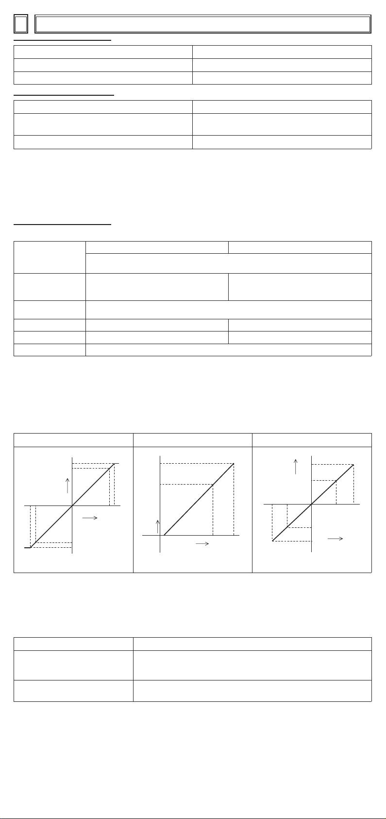
Preset 0 (-10V to +10V) Preset 1 (+4mA to +20mA) Preset 2 (-20mA to +20mA)
NOTE: Preset ranges are selected by an appropriate setting in buffer memory of the analog block.
Current/Voltage input selection must match the correct input terminal connections.
Miscellaneous
Item Specification
Isolation
Photo-coupler isolation between analog and digital circuits.
DC/DC converter isolation of power from FX
2N MPU.
No isolation between analog channels.
Number of occupied I/O points
8 points taken from the FX
2N expansion bus
(can be either inputs or outputs)
3.4 Allocation of buffer memories (BFM)
In buffer memory locations (BFMs)
marked with an “*” data can be written
from the PC using the TO command.
For buffer memories (BFMs) without “*”
mark, data can be read to the PC using
the FROM command.
Before reading from the analog special
function block, ensure these settings
have been sent to the analog special
function block. Otherwise, the previous
values held in the analog block will be
used.
The buffer memory also gives a facility
to adjust offset and gain by software.
Offset (intercept): The analog input
value when the digital output becomes 0.
Gain (slope): The analog input value
when the digital output becomes +1000.
(1) Channel Selection
Channel initialization is made by a 4 character HEX number HOOOO in buffer memory BFM #0.
The least significant character controls channel 1 and the 4 character controls channel 4.
Setting of each character is as follows:
O = 0: Preset range (-10V to +10V) O = 2: Preset range (-20mA to +20mA)
O = 1: Preset range (+4mA to +20mA) O = 3: Channel OFF
Example: H3310
CH1: Preset range (-10V to +10V)
CH2: Preset range (+4mA to +20mA)
CH3, CH4: Channel OFF
(2) Analog to Digital Conversion Speed Change
By writing 0 or 1 into BFM #15 of the FX
2N-4AD, the speed at which A/D conversion is performed can be changed.
However the following points should be noted:
To maintain a high speed conversion rate, use the FROM/TO commands as seldom as possible.
NOTES: When a conversion speed change is made, BFM #1-#4 are set to their default values immediately after the
change. This is regardless of the values they held originally. Bear this in mind if a speed change will be
made as part of the normal program execution.
(3) Adjusting Gain and Offset values
(a) When buffer memory BFM #20 is activated by setting it to K1, all settings within the analog special function
block are reset to their default settings. This is a very quick method to erase any undesired gain and offset
adjustments.
(b) If (b1, b0) of BFM #21 is set to (1,0), gain and offset adjustments are prohibited to prevent inadvertent changes
by the operator. In order to adjust the gain and offset values, bits (b1, b0) must be set to (0,1). The default is
(0,1).
(c) Gain and offset values of BFM #23 and #24 are sent to non-volatile memory gain and offset registers of the
specified input channels. Input channels to be adjusted are specified by the appropriate G-O (gain-offset) bits
of BFM #22
Example: If bits G1 and O1 are set to 1, input channel 1 will be adjusted when BFM #22 is written to by a TO
instruction.
(d) Channels can be adjusted individually or together with the same gain and offset values.
(e) Gain and offset values in BFM #23 #24 are in units of mV or µA. Due to the resolution of the unit the actual
response will be in steps of 5mV or 20µA.
FX2N-4AD SPECIAL FUNCTION BLOCK
USER’S GUIDE
JY992D65201B
TERMINAL LAYOUTS
2
BFM Contents
*#0 Channel initialization Default = H0000
*#1 Channel 1 Contains the number of samples (1 to
4096) to be used for an averaged result.
The default setting is 8-normal speed. High
speed operation can be selected with a
value of 1.
*#2 Channel 2
*#3 Channel 3
*#4 Channel 4
#5 Channel 1
These buffer memories contain the
averaged input values for the number of
samples entered for the channel in buffer
memories #1 to #4 respectively.
#6 Channel 2
#7 Channel 3
#8 Channel 4
#9 Channel 1
These buffer memories contain the present
value currently being read by each input
channel.
#10 Channel 2
#11 Channel 3
#12 Channel 4
#13-#14 Reserved
#15
Selection of A/D
conversion
speed see note 2
When set to 0, a normal speed is selected
of 15ms/ch (default)
When set to 1, a high speed is selected of
6ms/ch
BFM b7 b6 b5 b4 b3 b2 b1 b0
#16-#19 Reserved
*#20 Reset to Defaults and Preset. Default = 0
*#21 Offset, Gain Adjust Prohibit. Default = (0, 1) Permit
*#22 Offset, Gain Adjust G4 O4 G3 O3 G2 O2 G1 O1
*#23 Offset Value Default = 0
*#24 Gain Value Default = 5,000
#25-#28 Reserved
#29 Error status
#30 Identification code K2010
#31 Cannot be used
Voltage input
Digital output
-2,000
-2,048
-10.240V
+2,000
+2,047
+10.235V
+10V
-10V
+1,750
+1,000
Current input
Digital
output
+32mA
+20mA+4mA0
Current input
Digital
output
-1,000
-1,600
-32mA
+1,000
+1,600
+32mA
+20mA
-20mA
INTRODUCTION
1
INSTALLATION NOTES AND USAGE
3


 我的内容管理
展开
 我的资源
快来上传第一个资源
 我的收益 登录查看自己的收益
 我的积分
登录查看自己的积分
 我的C币
登录后查看C币余额
 我的收藏
我的收藏  我的下载
我的下载  下载帮助
下载帮助 
 前往需求广场,查看用户热搜

 信息提交成功