CDM10V 英飞凌芯片 INFINEON 中文版规格书手册.pdf
需积分: 5 86 浏览量
2023-07-11
09:40:32
上传
评论
收藏 1.2MB PDF 举报


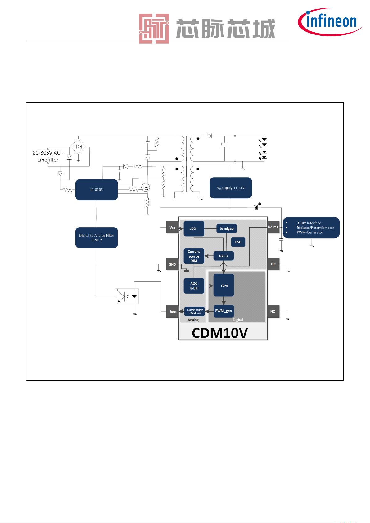
CDM10V
Flexible 0-10V Dimming Solution
Features
• Simplest 0-10 V design on the market. CDM10V comes with default settings:
- 5% minimum duty cycle
- 1kHz PWM frequency
- 200μA Dimmer/Resistor Bias current
- Dim-To-O disabled
• The simple one time programmable option allows setting in a wide range:
- Minimum duty cycle: 1%, 2%, 5%, 10%
- PWM output frequency: 200Hz, 500Hz, 1kHz, 2kHz
- Dimmer/Resistor Bias Current: 50μA, 100μA, 200μA, 500μA
- Dim-to-O: disabled/enabled
• Wide input V
cc
range from 11 to 25 V
• Transparent PWM mode (PWM Bypass Mode in DIM-TO-OFF enabled mode)
• Replaces many external components with a single chip reducing BOM and PCB space
• Minimum variation from device to device
Applications
• LED Drivers needing 0-10 V Dimming Circuits
• Industrial and Commercial Dimmable Applications:
Luminaires, Troers, Downlights, Sconces, Undercabinet, Oice Lighting, Signage applications,
Dali applications
Product Type Package
CDM10V SOT23-6
Description
CDM10V is a fully integrated 0-10 V dimming interface IC and comes in a SOT-23-6 package to cover space
requirements on small PCBs.
The device is targeted for various dimming applications in lighting. The IC can be used to transmit analog
voltage based signals from a 0-10 V dimmer or potentiometer to the dimming or PWM input of a lighting
controller IC in the form of a 5 mA current based PWM signal to drive an external opto-coupler. It replaces many
components in a traditional solution and reduces BOM and PCB space significantly.
The CDM10V IC outputs a 0 - 100% PWM current signal at programmable frequency with an amplitude value of 5
mA.
The duty cycle of the PWM signal can be limited to a dedicated minimum value. Dim-to-o feature is supported
as well and can be enabled on demand.
Embedded digital signal processing maintains minimum variations from device to device.
Please read the Important Notice and Warnings at the end of this document
v 1.3
www.infineon.com 2017-01-27


剩余19页未读,继续阅读
资源评论


