
Data Sheet 1 Rev. 1.2
www.infineon.com 2018-10-26
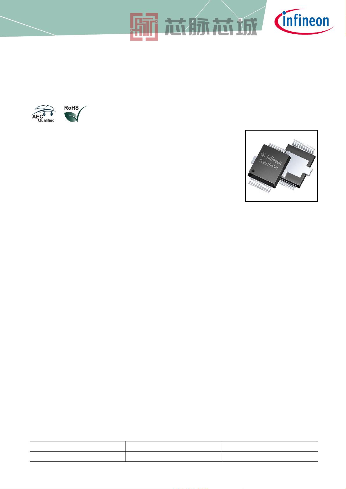
TLE9104SH
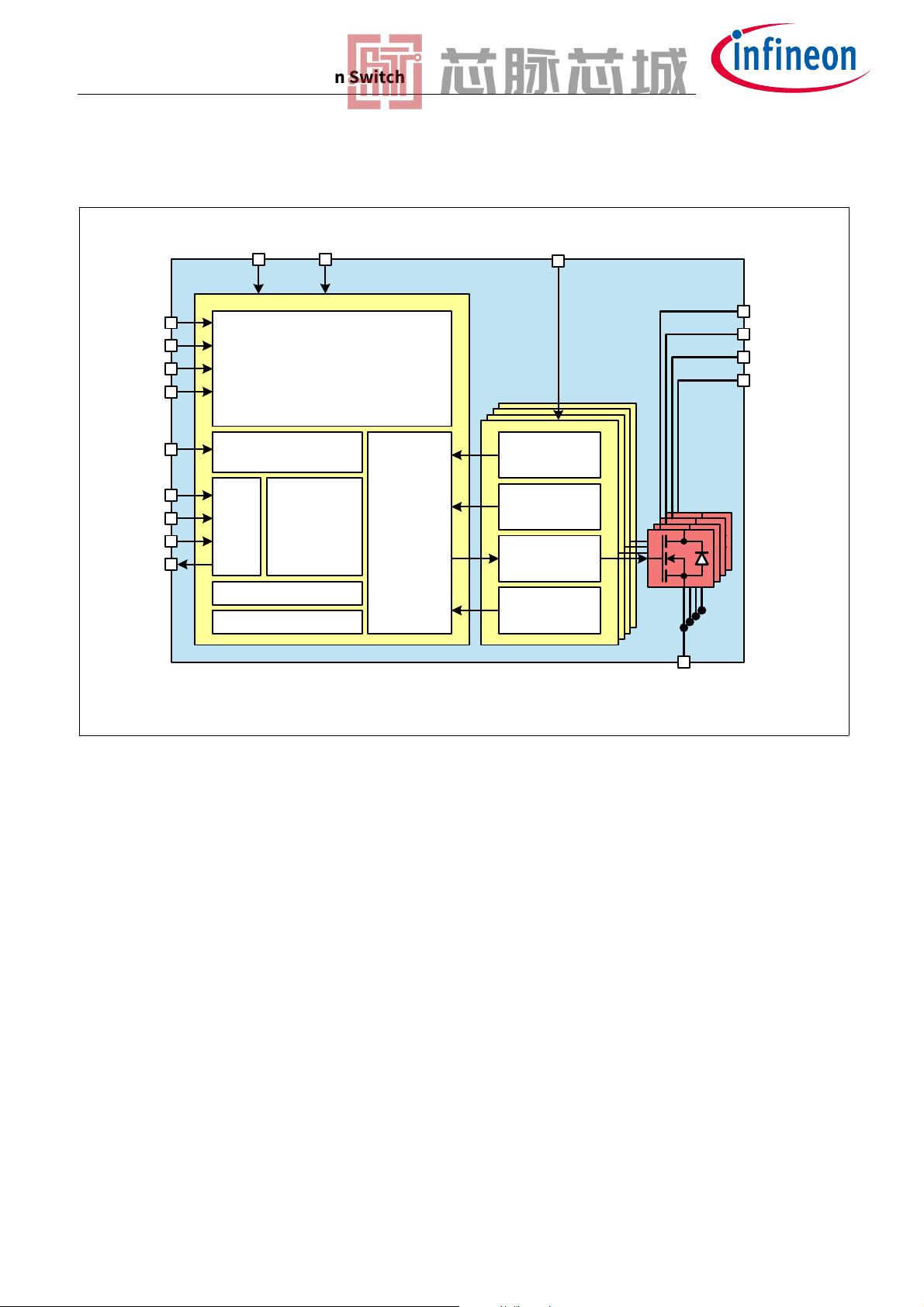
Smart Quad Channel Powertrain Switch
1 Overview
Features
• Configurable overcurrent protection
• Overtemperature protection
•Open load detection
• Short circuit to GND detection
• Electrostatic Discharge (ESD) protection
• 16-Bit SPI (for diagnostic and control)
• Soldering: Automated Optical Inspection capability (AOI)
• Green product (completely lead free)
• AEC qualified
Potential applications
The TLE9104SH is best suited for Automotive Powertrain applications. It can be used as driver IC for inductive
and ohmic actuators such as injectors, solenoids and relays.
Product validation
Qualified for Automotive Applications. Product Validation according to AEC-Q100/101.
Description
Quad Low-Side Switch in Smart Power Technology (SPT) with four open drain DMOS output stages. The
TLE9104SH is protected by embedded protection functions and designed for automotive powertrain
applications. The output stages can be controlled directly by parallel inputs for PWM applications (for
example gasoline multiport injection) or by SPI.
Type Package Marking
TLE9104SH PG-DSO-20-88 TLE9104SH


剩余34页未读,继续阅读
资源评论


芯脉芯城
- 粉丝: 4
- 资源: 4030


最新资源
- 基于微信小程序的网上商城+ssm-微信小程序毕业项目,适合计算机毕-设、实训项目、大作业学习.rar
- 教学辅助微信小程序设计+ssm-微信小程序毕业项目,适合计算机毕-设、实训项目、大作业学习.rar
- 基于微信小程序的童装商城的设计与实现+ssm-微信小程序毕业项目,适合计算机毕-设、实训项目、大作业学习.rar
- Python 实现GARCH分位数时间序列预测的设计项目实例(含完整的程序,GUI设计和代码详解)
- 家庭记账本的设计与实现+ssm-微信小程序毕业项目,适合计算机毕-设、实训项目、大作业学习.rar
- 基于微信小程序的校园二手交易平台系统设计与开发ssm-微信小程序毕业项目,适合计算机毕-设、实训项目、大作业学习.rar
- 基于微信小程序的小区疫情防控ssm-微信小程序毕业项目,适合计算机毕-设、实训项目、大作业学习.rar
- 流浪动物救助小程序--论文pf-微信小程序毕业项目,适合计算机毕-设、实训项目、大作业学习.zip
- 开放实验室预约管理系统pf-微信小程序毕业项目,适合计算机毕-设、实训项目、大作业学习.zip
- 美食推荐系统的微信小程序--论文pf-微信小程序毕业项目,适合计算机毕-设、实训项目、大作业学习.zip
- 基于小程序的社区超市管理系统springboot-微信小程序毕业项目,适合计算机毕-设、实训项目、大作业学习.rar
- 基于微信小程序的在线选课系统springboot-微信小程序毕业项目,适合计算机毕-设、实训项目、大作业学习.rar
- 生活小助手微信小程序_k1s0l-微信小程序毕业项目,适合计算机毕-设、实训项目、大作业学习.zip
- 农场管理系统(小程序)--论文pf-微信小程序毕业项目,适合计算机毕-设、实训项目、大作业学习.zip
- 基于微信小程序的学生公寓电费信息管理系统+ssm-微信小程序毕业项目,适合计算机毕-设、实训项目、大作业学习.rar
- 农业电商服务系统_30249--论文-微信小程序毕业项目,适合计算机毕-设、实训项目、大作业学习.zip
资源上传下载、课程学习等过程中有任何疑问或建议,欢迎提出宝贵意见哦~我们会及时处理!
点击此处反馈


