TL1451 友顺UTC 电子元器件芯片.pdf
需积分: 5 131 浏览量
2023-05-30
09:58:31
上传
评论
收藏 619KB PDF 举报

UNISONIC TECHNOLOGIES CO., LTD
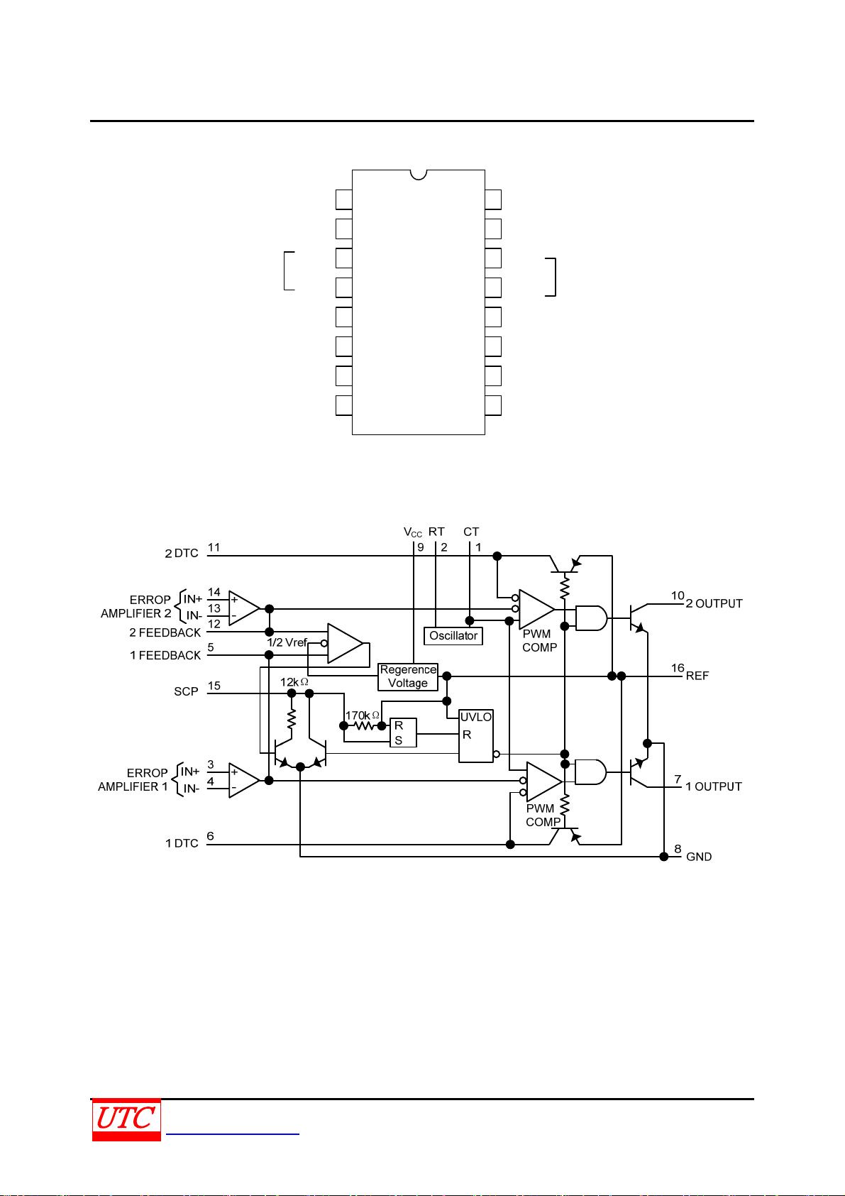
TL1451
LINEAR INTEGRATED CIRCUIT
1 of 14
Copyright © 2015 Unisonic Technologies Co., Ltd
QW-R103-011.F
DUAL
PULSE-WIDTH-MODULATION
CONTROL CIRCUITS
DESCRIPTION
The UTC TL1451 incorporates on a single monolithic chip all
the functions required in the construction of two
pulse-width-modulation (PWM) control circuits. Designed primarily
for power supply control, the UTC TL1451 contains an on-chip
2.5V regulator, two error amplifiers, an adjustable oscillator, two
dead-time comparators, undervoltage lockout circuitry, and dual
common –emitter output transistor circuits.
FEATURES
*Complete PWM power control circuitry
*Completely synchronized operation
*Internal undervoltage lockout protection
*Wide supply voltage range
*Internal Short-Circuit protection
*Oscillator frequency 500kHz max
*Variable dead time provides control over total range
*Internal regulator provides a stable 2.5V reference supply
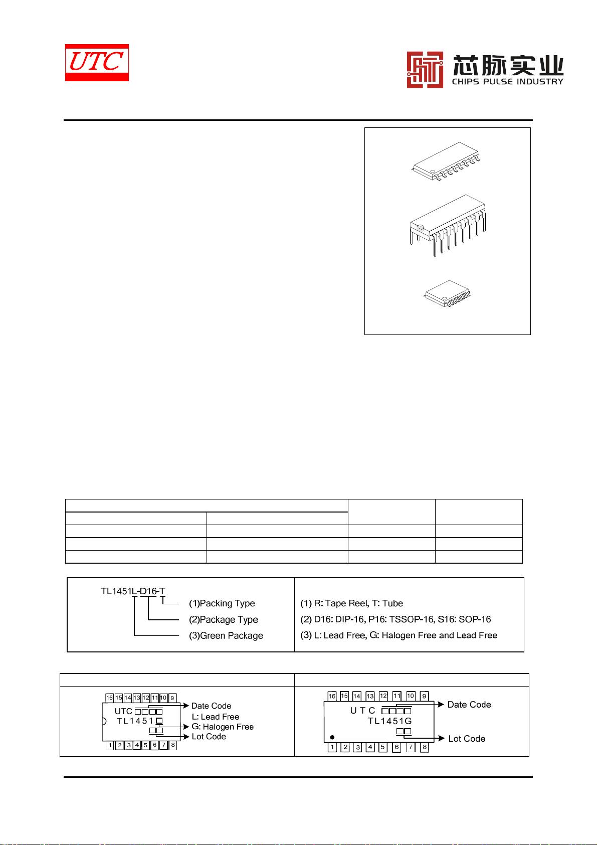
DIP-16
SOP-16
TSSOP-16
ORDERING INFORMATION
Ordering Number
Lead Free Halogen Free
Package Packing
TL1451L-D16-T TL1451G-D16-T DIP-16 Tube
- TL1451G-P16-R TSSOP-16 Tape Reel
- TL1451G-S16-R SOP-16 Tape Reel
MARKING
DIP-16 SOP-16 / TSSOP-16
剩余13页未读,继续阅读
资源评论


