没有合适的资源?快使用搜索试试~ 我知道了~
CH7033B Full Datasheet Rev1.32
需积分: 10 14 下载量 64 浏览量
2018-08-21
20:25:02
上传
评论 1
收藏 1.48MB PDF 举报
温馨提示
试读
46页
CH7033B Full Datasheet Rev1.32,详细手册,包括寄存器配置值。
资源推荐
资源详情
资源评论
CH7033B
Full datasheet
201-1000-024 Rev1.32 04/11/2016 1
Chrontel
CH7033B HDTV/VGA/DVI Encoder
FEATURES
GENERAL DESCRIPTION
DVI encoder support up to 1080p
Supports Component YPrPb (HDTV) up to 1080p
and analog RGB (VGA) monitor up to 1920x1080
resolution
Support scaled and bypassed video streams output
from VGA/HDTV and DVI interfaces
simultaneously
Three 10-bit high speed DACs
SPDIF audio interface supports either 16-bit or 20-
bit stereo data for up to 192kHz/2ch
Support 2 channel I2S digital audio input for up to
24-bit data stream (32kHz, 44.1kHz, 48kHz,
88.2kHz, 96kHz, 176.4kHzand 192kHz)
DDC master for reading EDID
Hot plug detection for DVI
TV/Monitor connection detect capability. DACs can
be switched off through programming internal
registers
Pixel-level color enhancement for brightness,
contrast, hue and saturation adjustment for HDTV
and VGA output
On-chip frame buffer supports frame rate conversion
provides the graphic controller the flexibility of
video timing output
Advanced scaling engine to upsize/downsize input
resolution for DVI display up to 1080p, VGA up to
1920 x1080 and HDTV up to 1080p
Supports 8/12/16/18/24-bit parallel interface input
for either RGB format (RGB-565, RGB-666 or
RGB-888 and etc.) or YCrCb format (ITU-R 656 or
ITU-R 601). 80/86 MPU interface and DE only
mode are also supported.
Wide range of input resolutions support for up to
1366x768 (i.e. 640x480, 720x480, 720x576,
800x600, 1024x600, 1024x768, 1280x800, and etc.)
Image display rotation support at 90/180/270 degree
or flipped in horizontal/vertical position
Pixel clock input frequency support for up to 165
MHz
IO Supply Voltages from 1.2V to 3.3V and
SPC/SPD Supply Voltages from 1.8V to 3.3V.
Programmable power management
Device fully programmable through serial port or
can automatically load firmware from Chrontel Boot
ROM (CH9904)
Offered in a 88-pin QFN package
The Chrontel CH7033B is specifically designed for
consumer electronics device and PC markets which
multiple high definition content display formats are
required. With its advanced video encoder, flexible
scaling engine and easy-to-configure audio interface, the
CH7033B satisfies manufactures’ products display
requirements and reduce their costs of development and
time-to-market.
High quality high-bandwidth uncompressed video like
DVI and YPrPb components or legacy VGA analog
display are supported by the device’s color format
converter. The 3 high-performance, 10-bit DACs can be
used for either HDTV display or VGA output depending
on manufactures’ products specification. The device is
compliant with EIA770-3 and SMPTE
274M/293M/296M standards and supports HDTV
resolution for up to 1080p. The CH7033B has the ability
to generate composite syncs if required by the RGB
monitor.
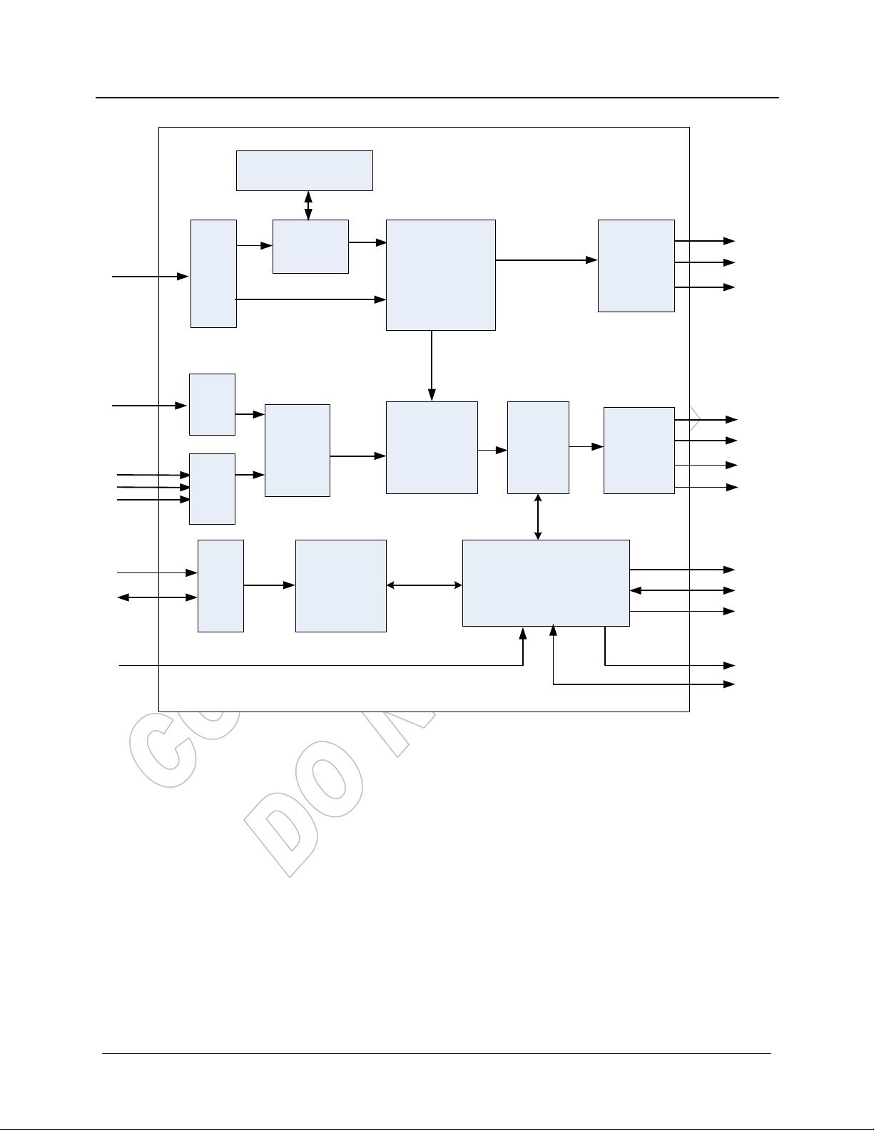
The CH7033B’s 24-bit parallel bus accepts a wide range
of input data formats from the graphic controller. The
built-in video port supports 8/12/16/18/24-bit data
interface as well as 80/86 MPU interface. The video
format conversion module is capable of translating digital
RGB-565, RGB-666, RGB-888 or YCrCb (ITU-R 656,
ITU-R 601) signal to the DVI signal, combining with the
audio stream. The input digital signal also can be
transformed by the DACs for HDTV or VGA analog
outputs. The device’s video capture block supports input
display resolution for up to 1366x768 which can be either
interlaced or non-interlaced timing.
The CH7033B has incorporated a high speed SDRAM
that allows manufactures to design their products to
achieve simultaneous display digital signal and analog
signal. Leverage the benefit of the framebuffer, the
device’s sophisticated scaler is able to produce two same
video content, which will be routed to separate output
driver for display. Frame Rate Conversion is embedded
in the scaler; it can maximize the native input resolution
up to 1080p for HD display. Furthermore the CH7033B
provides additional image manipulation features
including image rotation that can be controlled through
programming internal registers.
The CH7033B supports both SPDIF and 2-channel I²S
CHRONTEL CH7033B
2 201-1000-024 Rev1.32 04/11/2016
APPLICATION
Media Internet Devices
Media Storage Boxes
Smart-books
Digital Video Players
Digital Video Recorders
Portable Media Players
digital audio input. Its high fidelity audio decoder engine
has the capability of sampling audio frequency for up to
192k/2ch. The SPIDF supports PCM encoded data and
compressed audio including Dolby Digital and DTS.
The CH7033B has an image enhancement function that
can fine tune brightness, contrast, hue and saturation
down to the pixel-level.
When the HPD signal is asserted, the CH7033B will
automatically generate an interrupt to the processor. A
build-in DDC port can read the EDID data from DVI
monitor through programming. registers by the processor.
CHRONTEL CH7033B
201-1000-024 Rev1.32 04/11/2016 3
Input
format
decoder
Scaler
SDRAM
Mix video and audio
Audio packet
org
SPDIF
decoder
I2S_CK
I2S_WS
I2S_D
TMDS
(TERC4)
encoder
Differential
serializer
EDID MCU
I2C slave
Registers,
EDID buffer
SPC
SPD
HPD
DDC_SC
DDC_SD
TLC*/TLC
TDC0*/TDC0
TDC1*/TDC1
TDC2*/TDC2
IRQ
DAC
DAC0
DAC1
DAC2
SPCM
SPDM
D[23:0]
I2S
decoder
SPDIF
Video
Format
Figure 1: Functional Block Diagram
CHRONTEL CH7033B
4 201-1000-024 Rev1.32 04/11/2016
TABLE OF CONTENTS
FEATURES ....................................................................................................................................... 1
GENERAL DESCRIPTION ................................................................................................................. 1
APPLICATION .................................................................................................................................. 2
1.0 PIN-OUT ............................................................................................................................ 6
1.1 Package Diagram ........................................................................................................................................... 6
1.2 Pin Description .............................................................................................................................................. 7
2.0 FUNCTIONAL DESCRIPTION ............................................................................................ 10
2.1 Video Input .................................................................................................................................................. 10
2.1.1 Overview ............................................................................................................................................. 10
2.1.2 Input Clock and Data Timing Diagram................................................................................................ 10
2.1.3 Input data voltage ................................................................................................................................ 11
2.1.4 Input data format .................................................................................................................................. 12
2.2 Audio Input .................................................................................................................................................. 13
2.2.1 SPDIF Input ......................................................................................................................................... 13
2.2.2 I2S Input .............................................................................................................................................. 13
2.3 DAC Output ................................................................................................................................................. 14
2.3.1 HDTV Output ...................................................................................................................................... 14
2.3.2 VGA Output......................................................................................................................................... 14
2.3.3 DAC output Configuration .................................................................................................................. 15
2.3.4 DAC single/double termination ........................................................................................................... 15
2.3.5 TV connection detect ........................................................................................................................... 15
2.3.6 Picture enhancement ............................................................................................................................ 15
2.4 DVI Output .................................................................................................................................................. 15
2.5 EDID Buffer ................................................................................................................................................ 17
2.6 Testing Functions and Power Down Mode .................................................................................................. 17
2.6.1 Test Pattern Select ............................................................................................................................... 17
2.6.2 SDRAM Power Down ......................................................................................................................... 17
3.0 REGISTER CONTROL ....................................................................................................... 19
3.1 Control Registers Map ................................................................................................................................. 19
3.2 Register Descriptions ................................................................................................................................... 21
4.0 ELECTRICAL SPECIFICATIONS ........................................................................................ 41
4.1 Absolute Maximum Ratings ........................................................................................................................ 41
4.2 Recommended Operating Conditions .......................................................................................................... 41
4.3 Electrical Characteristics ............................................................................................................................. 42
4.4 Digital Inputs / Outputs DC Specifications.................................................................................................. 42
4.5 Digital Inputs / Outputs AC Specifications................................................................................................. 43
4.6 TMDS Output Specification ........................................................................................................................ 43
5.0 PACKAGE DIMENSIONS ................................................................................................... 44
6.0 REVISION HISTORY ......................................................................................................... 45
CHRONTEL CH7033B
201-1000-024 Rev1.32 04/11/2016 5
FIGURES AND TABLES
LIST OF FIGURES
Figure 1: Functional Block Diagram ............................................................................................................................. 3
Figure 2: 88 pin QFN Package (Top View) ................................................................................................................... 6
Figure 3: Clock and Data Input Timing in 3x Multiplexed Mode ............................................................................... 10
Figure 4: SDR and DDR Input Data Formats .............................................................................................................. 10
Figure 5: Horizontal Input Timing............................................................................................................................... 11
Figure 6: Vertical Input Timing ................................................................................................................................... 11
Figure 7: 80/86 MPU Interface Timing ....................................................................................................................... 11
Figure 8: SPDIF interface format ................................................................................................................................ 13
Figure 9: I2S interface format ...................................................................................................................................... 14
Figure 10: 88 Pin QFN Package (10 x 10 mm) ........................................................................................................... 44
LIST OF TABLES
Table 1: Pin Name Descriptions (QFN88 Package) ...................................................................................................... 7
Table 2: Input data format .......................................................................................................................................... 12
Table 3: Supported HDTV standards........................................................................................................................... 14
Table 4: Composite sync type ...................................................................................................................................... 14
Table 5: Video DAC Configurations for CH7033B .................................................................................................... 15
Table 6: video formats the CH7033B supports........................................................................................................... 16
Table 7: DVI output formats the CH7033B supports .................................................................................................. 16
Table 8: Popular panel size .......................................................................................................................................... 17
Table 9: Test Pattern Selection .................................................................................................................................... 17
Table 10: Serial Port Register Map ............................................................................................................................. 19
Table 11: SYNC SWAP .............................................................................................................................................. 29
Table 12: VGA Output format ..................................................................................................................................... 30
Table 13: HDTV output format ................................................................................................................................... 30
Table 14: Video DAC Configurations for CH7033 ..................................................................................................... 34
Table 15: TEST PATTERN......................................................................................................................................... 35
Table 16: TMDS output specification ......................................................................................................................... 43
剩余45页未读,继续阅读
资源评论
wubangqiang
- 粉丝: 2
- 资源: 1
上传资源 快速赚钱
- 我的内容管理 展开
- 我的资源 快来上传第一个资源
- 我的收益 登录查看自己的收益
- 我的积分 登录查看自己的积分
- 我的C币 登录后查看C币余额
- 我的收藏
- 我的下载
- 下载帮助
最新资源
- DrawDB 是一个健壮且用户友好的数据库实体关系 (DBER) 编辑器,直接位于您的浏览器中
- PHP库通过返回原始SQL来实现ActiveRecord 用于PHP5.3和NO PDO场景的yii2 ORM移植
- 5152单片机proteus仿真和源码用数组作函数参数控制流水花样
- 2024年全域电商矩阵109节线上课-课程网盘链接提取码下载 .txt
- 对 sqlite 的使用进行简单封装,仅涉及简单的单表 增删改查,基于 FMDB, 操作基于 model
- 5152单片机proteus仿真和源码用函数型指针控制P1口灯花样
- 对Hibernate框架的二次封装,简化对数据库的操作
- 5152单片机proteus仿真和源码用定时器T1查询方式控制单片机发出1KHz音频
- 由 Top10 开发和使用的惯用 Scala Redis 客户端 这是一项正在进行的工作,虽然在生产中使用,但应将其视为在生产中
- SwiftUI - SceanAppDelegate
资源上传下载、课程学习等过程中有任何疑问或建议,欢迎提出宝贵意见哦~我们会及时处理!
点击此处反馈
安全验证
文档复制为VIP权益,开通VIP直接复制
信息提交成功