MAX1483数据手册
需积分: 34 191 浏览量
2012-12-05
22:02:02
上传
评论
收藏 173KB PDF 举报

_______________General Description
The MAX1482 and MAX1483 are low-power trans-
ceivers for RS-485 and RS-422 communication. Both
feature slew-rate-limited drivers that minimize EMI and
reduce reflections caused by improperly terminated
cables. Data rates are guaranteed up to 250kbps.
The MAX1482/MAX1483 draw only 20µA of supply cur-
rent. Additionally, they have a low-current shutdown
mode that consumes only 0.1µA. Both parts operate
from a single +5V supply.
Drivers are short-circuit current limited and are protect-
ed against excessive power dissipation by thermal
shutdown circuitry that places the driver outputs into a
high-impedance state. The receiver input has a fail-safe
feature that guarantees a logic-high output if the input
is open circuit.
The MAX1482 is full duplex and the MAX1483 is half
duplex. Both parts have a
1
⁄
8
-unit-load input impedance
that guarantees up to 256 transceivers on the bus.
________________________Applications
Low-Power RS-485/RS-422 Networks
Transceivers for EMI-Sensitive Applications
Industrial-Control Local Area Networks
Large 256-Node LANs
____________________________Features
♦ Low 20µA Operating Current
♦ Slew-Rate Limited for Reduced EMI and
Reduced Reflections
♦ 0.1µA Low-Current Shutdown Mode
♦ Designed for RS-485 and RS-422 Applications
♦ Operate from a Single +5V Supply
♦ -7V to +12V Common-Mode Input Voltage Range
♦ Allows up to 256 Transceivers on the Bus—
Guaranteed (
1
⁄
8
-unit load)
♦ Current Limiting and Thermal Shutdown for
Driver Overload Protection
______________Ordering Information
MAX1482/MAX1483
20µA,
1
⁄
8
-Unit-Load, Slew-Rate-Limited
RS-485 Transceivers
________________________________________________________________
Maxim Integrated Products
1
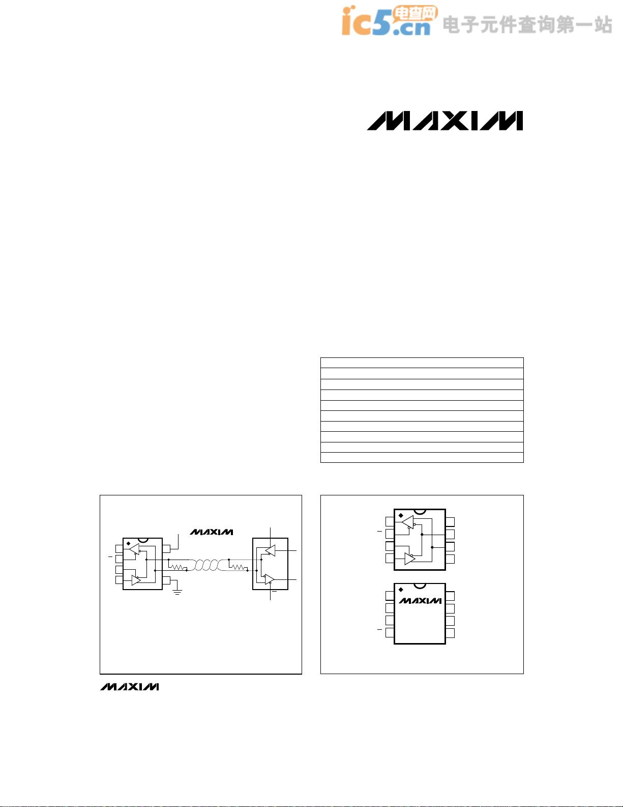
TOP VIEW
1
2
3
4
8
7
6
5
V
CC
B
A
GND
DI
DE
RE
RO
DIP/SO
R
D
1
2
3
4
8
7
6
5
V
CC
A
GND
DE
RE
B
RO
µMAX
DI
MAX1483
_________________Pin Configurations
MAX1483
NOTE: PIN LABELS Y AND Z ON TIMING, TEST, AND WAVEFORM
DIAGRAMS REFER TO PINS A AND B WHEN DE IS HIGH.
TYPICAL OPERATING CIRCUIT SHOWN WITH DIP/SO PACKAGE.
1
2
3
4
8
5
V
CC
+5V
GND
DI
DE
RE
RO
R
D
Rt
Rt
7
6
D
R
DE
RE
DI
RO
A
B
B
A
_________Typical Operating Circuits
Call toll free 1-800-998-8800 for free samples or literature.
19-0367; Rev 0; 2/95
PART
MAX1482CPD
MAX1482CSD
MAX1482EPD -40°C to +85°C
0°C to +70°C
0°C to +70°C
TEMP. RANGE PIN-PACKAGE
14 Plastic DIP
14 SO
14 Plastic DIP
MAX1482ESD -40°C to +85°C 14 SO
MAX1483CPA
0°C to +70°C 8 Plastic DIP
MAX1483CSA 0°C to +70°C 8 SO
MAX1483CUA 0°C to +70°C 8 µMAX
MAX1483EPA -40°C to +85°C 8 Plastic DIP
MAX1483ESA -40°C to +85°C 8 SO
MAX1482 appears at end of data sheet.
MAX1482 appears at end of data sheet.
剩余12页未读,继续阅读
资源评论


