IEEE TRANSACTIONS ON CIRCUITS AND SYSTEMS—I: FUNDAMENTAL THEORY AND APPLICATIONS, VOL. 48, NO. 9, SEPTEMBER 2001 1041
Analysis of Multistage Amplifier–Frequency
Compensation
Ka Nang Leung and Philip K. T. Mok, Member, IEEE
Abstract—Frequency-compensation techniques of single-, two-
and three-stage amplifiers based on Miller pole splitting and
pole–zero cancellation are reanalyzed. The assumptions made,
transfer functions, stability criteria, bandwidths, and important
design issues of most of the reported topologies are included.
Several proposed methods to improve the published topologies
are given. In addition, simulations and experimental results are
provided to verify the analysis and to prove the effectiveness of
the proposed methods.
Index Terms—Damping-factor-control frequency compen-
sation, multipath nested Miller compensation, multipath zero
cancellation, multistage amplifier, nested Gm-C compensation,
nested Miller compensation, simple Miller compensation.
I. INTRODUCTION
M
ULTISTAGE amplifiers are urgently needed with the
advance in technologies, due to the fact that single-stage
cascode amplifier is no longer suitable in low-voltage designs.
Moreover, short-channel effect of the sub-micron CMOS
transistor causes output-impedance degradation and hence
gain of an amplifier is reduced dramatically. Therefore, many
frequency-compensation topologies have been reported to
stabilize the multistage amplifiers [1]–[26]. Most of these
topologies are based on pole splitting and pole–zero can-
cellation using capacitor and resistor. Both analytical and
experimental works have been given to prove the effectiveness
of these topologies, especially on two-stage Miller compen-
sated amplifiers. However, the discussions in some topologies
are focused only on the stability criteria, but detailed design
information such as some important assumptions are missing.
As a result, if the provided stability criteria cannot stabilize
the amplifier successfully, circuit designers usually choose the
parameters of the compensation network by trial and error and
thus optimum compensation cannot be achieved.
In fact, there are not many discussions on the comparison of
the existingcompensationtopologies. Therefore, the differences
as well as the pros and cons of the topologies should be inves-
tigated in detail. This greatly helps the designers in choosing a
suitable compensation technique for a particular design condi-
tion such as low-power design, variable output capacitance or
variable output current.
Manuscript received March 9, 2000; revised February 6, 2001. This work
was supported by the Research Grant Council of Hong Kong, China under grant
HKUST6007/97E. This paper was recommended by Associate Editor N. M. K.
Rao.
The authorsarewith the Department of Electrical and Electronic Engineering,
The Hong Kong University of Science and Technology, Clear Water Bay, Hong
Kong (e-mail: eemok@ee.ust.hk).
Publisher Item Identifier S 1057-7122(01)07716-9.
Moreover, practical considerations on the compensation tech-
niques of
-stage amplifiers are questionable since any extra
stage consumes more power, requires more complicated circuit
structure and may reduce the bandwidth dramatically. In fact,
the three-stage amplifier provides sufficient dc gain for most ap-
plications, and, therefore, frequency-compensation techniques
for amplifiers with up to three stages are sufficient and worth-
while to develop.
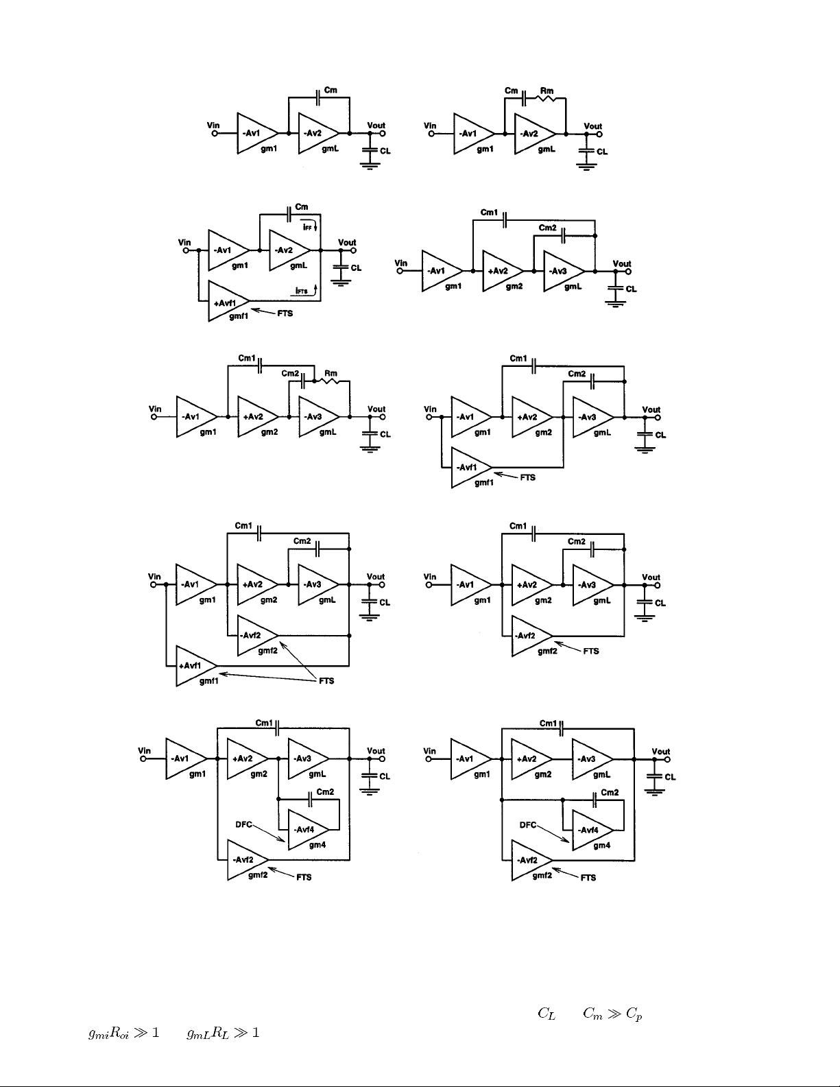
Regarding these issues, this paper firstly gives a review on
single-stageamplifierinSectionIIIandthenaddressessomepub-
lished topologies for two- and three-stage amplifiers from Sec-
tions IV to VIII, including simple Miller compensation (SMC),
multipath zero cancellation (MZC), nested Miller compensation
(NMC), multipath NMC (MNMC), nested Gm-C compensation
(NGCC), and damping-factor-control frequency-compensation
(DFCFC). Especially, single-end amplifiers are used to discuss
the compensation topologies. The assumptions made, transfer
functions, stability criteria, and design considerations are given.
Several proposed methods to eliminate some design problems
are also included with the support of simulations and experi-
mental results. A summary, a comparison and some important
issues of the studied topologies are given in Section IX. Finally,
a discussion on the robustness of the studied compensation tech-
niques is included.
II. N
OTATIONS DECLARATION AND ASSUMPTIONS
In this section, the general notations used in this paper are
firstly defined, then the common assumptions in all topologies
are stated.
1) Notations Declaration:
, , and are defined as
the transconductance, output resistance and lumped output para-
sitic capacitance of the
th gain stage, respectively. Particularly,
is the output stage transconductance, is the loading re-
sistance and
is the loading capacitance. The compensation
capacitor is denoted by
. The voltage-gain transfer func-
tion is defined as
where and
are the input and output signal voltage, respectively. Moreover,
GBW stands for the gain-bandwidth product and PM for the
phase margin.
2) Assumptions: Due to the complicated compensation
structures, the transfer functions are generally very complicated
and cannot be analyzed easily. In this case, analysis with
numerical method using computers is feasible. However, this
loses the insight on some critical parameters to improve the
frequency response. Therefore, some assumptions are made
here to simplify the transfer functions without losing the
1057–7122/01$10.00 © 2001 IEEE
Authorized licensed use limited to: Peking University. Downloaded on August 11, 2009 at 04:48 from IEEE Xplore. Restrictions apply.


 xuxianming1112012-08-06比较深奥 我看不太懂
 我的内容管理
展开
 我的资源
快来上传第一个资源
 我的收益 登录查看自己的收益
 我的积分
登录查看自己的积分
 我的C币
登录后查看C币余额
 我的收藏
我的收藏  我的下载
我的下载  下载帮助
下载帮助 
 前往需求广场,查看用户热搜

 信息提交成功