8051 IP Core
Bootstrap Demo Design - User Guide
Erfolg folgt Erfahrung
Implementing the MC8051 IP Core On A Cyclone Nios Board
First of all it is necessary to exchange the simulation models of all the memory blocks with
real memory that can be found inside the target FPGA. It is also recommended to implement a
PLL to get a clock signal with a lower frequency than that of the on-board oscillator. The
VHDL code for these entities is generated by the backend tool, i.e. Quartus II 4.0 for Altera
FPGAs.
Step 1: Choose the function that should be generated.
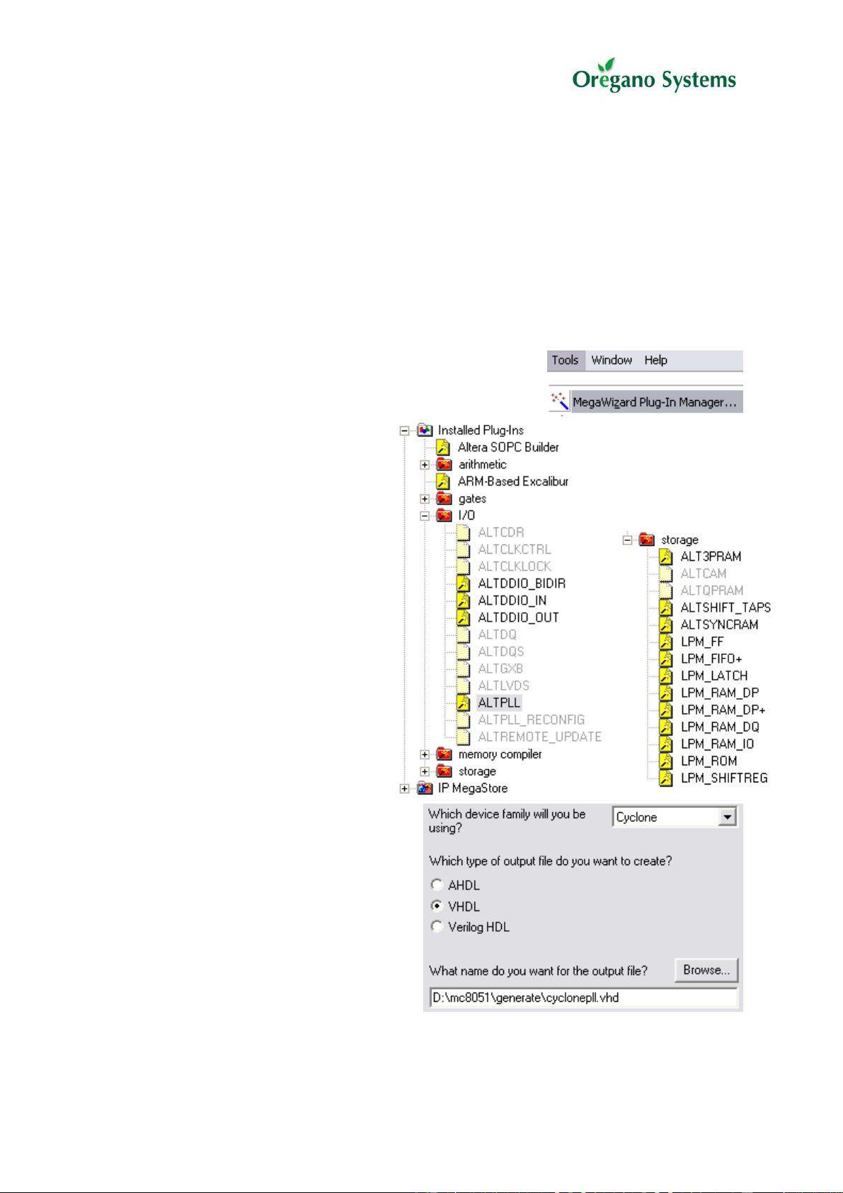
1. After starting Quartus II, launch the Megawizard
Plug-In Manager that is located in the Tools-Menu.
2. Select the function block that
should be generated.
The PLL will be designed first.
This function can be found in the
I/O folder and is named ALTPLL.
In a second turn the memories
will be drawn. The functions for
those blocks can be found in the
folder named storage. It contains
the functions LPM_ROM for the
mc8051_rom entity and
LPM_RAM_DQ for the entity
mc8051_ram and mc8051_ramx
respectively.
3. Set the device family to Cyclone.
Then choose the language of the
HDL output file.
Finally the name of the output file
and its destination directory must
be set. It is recommended to store
all code files belonging to FPGA
functions in a directory named
generate.
Copyright © 2004 – All rights reserved http://oregano.at


