TI-TMS626812B.pdf
需积分: 0 58 浏览量
2022-12-10
22:58:36
上传
评论 4
收藏 611KB PDF 举报

TMS626812B
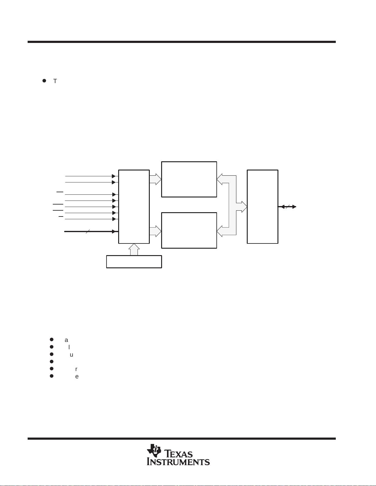
1 048 576 BY 8-BIT BY 2-BANK
SYNCHRONOUS DYNAMIC RANDOM-ACCESS MEMORIES
SMOS693A – OCTOBER 1997 – REVISED APRIL 1998
1
POST OFFICE BOX 1443 • HOUSTON, TEXAS 77251–1443
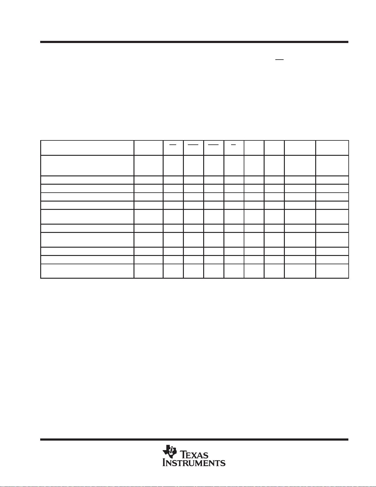
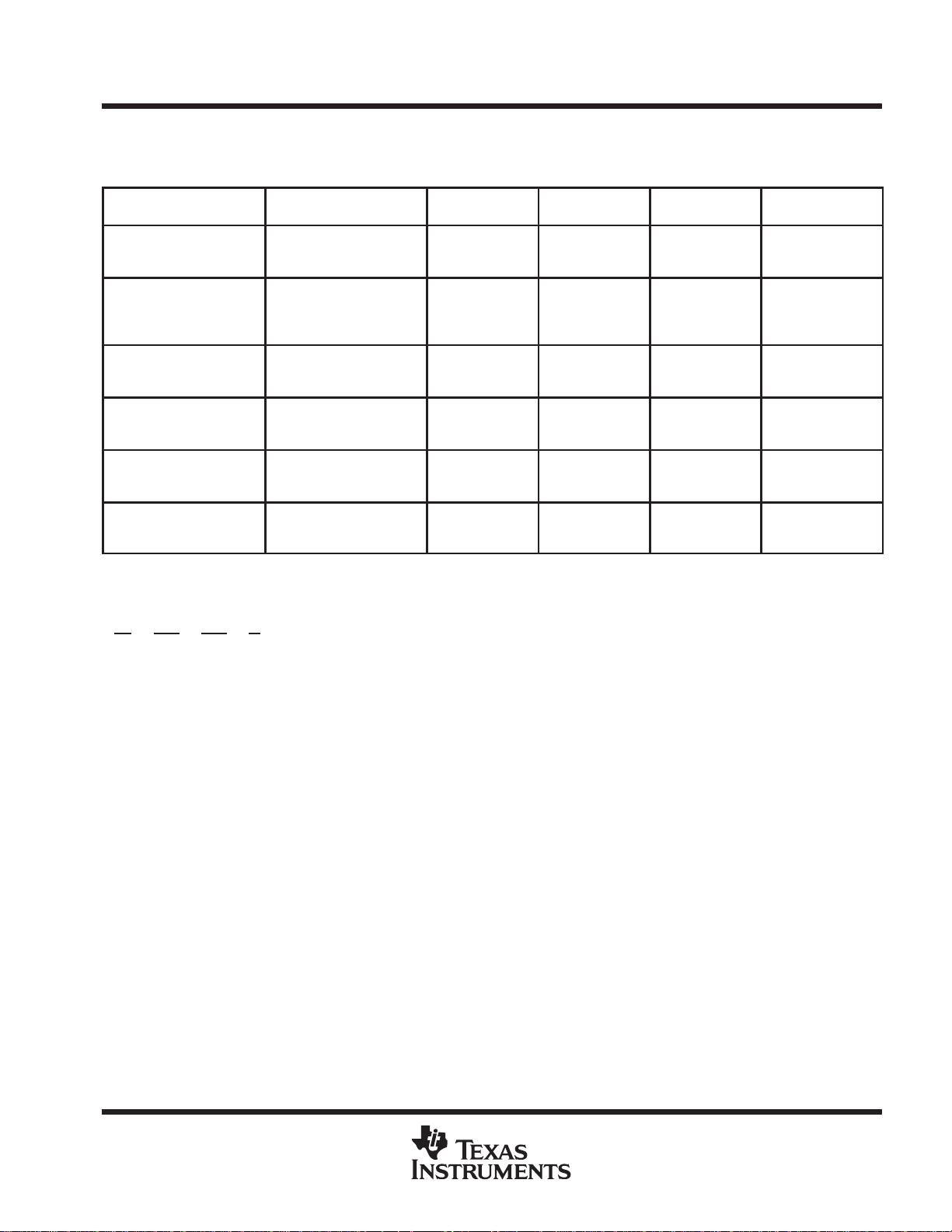
SYNCHRONOUS
CLOCK
CYCLE TIME
ACCESS TIME
(CLOCK TO
OUTPUT)
REFRESH
TIME
INTERVAL
t
CK3
(CL
†
=3)
t
CK2
(CL=2)
t
AC3
(CL=3)
t
AC2
(CL=2)
’626812B-8 8 ns 10 ns 6 ns 6 ns 64 ms
’626812B-8A 8 ns 15 ns 6 ns 7 ns 64 ms
’626812B-10 10 ns 15 ns 7.5 ns 7.5 ns 64 ms
†
CL = CAS latency
Please be aware that an important notice concerning availability, standard warranty, and use in critical applications of
Texas Instruments semiconductor products and disclaimers thereto appears at the end of this data sheet.
D
Organization
1048576 by 8 Bits by 2 Banks
D
3.3-V Power Supply (±10% Tolerance)
D
Two Banks for On-Chip Interleaving
(Gapless Accesses)
D
High Bandwidth – Up to 125-MHz Data
Rates
D
CAS Latency (CL) Programmable to
2 or 3 Cycles From Column-Address Entry
D
Burst Sequence Programmable to Serial or
Interleave
D
Burst Length Programmable to 1, 2, 4, or 8
D
Chip Select and Clock Enable for Enhanced
System Interfacing
D
Cycle-by-Cycle DQ Bus Mask Capability
D
Auto-Refresh and Self-Refresh Capabilities
D
4K Refresh (Total for Both Banks)
D
High-Speed, Low-Noise, Low-Voltage TTL
(LVTTL) Interface
D
Power-Down Mode
D
Compatible With JEDEC Standards
D
Pipeline Architecture
D
Temperature Ranges
Operating, 0°C to 70°C
Storage, – 55°C to 150°C
D
Intel PC100 Compliant (-8A, -8, and
-10 Devices)
D
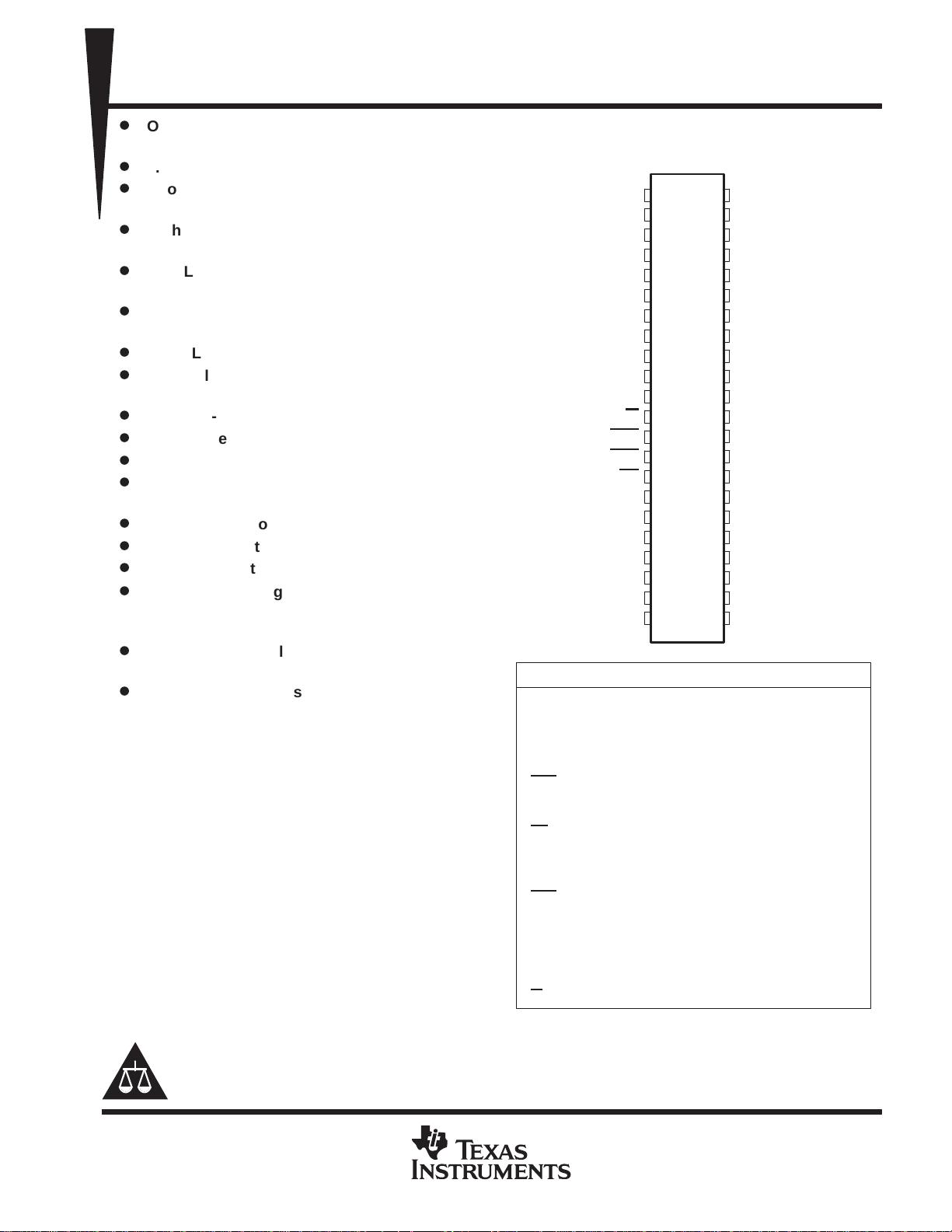
Performance Ranges:
44
43
42
41
40
39
38
37
36
35
34
33
32
31
30
29
28
27
26
25
24
23
V
SS
DQ7
V
SSQ
DQ6
V
CCQ
DQ5
V
SSQ
DQ4
V
CCQ
NC
NC
DQM
CLK
CKE
NC
A9
A8
A7
A6
A5
A4
V
SS
1
2
3
4
5
6
7
8
9
10
11
12
13
14
15
16
17
18
19
20
21
22
V
CC
DQ0
V
SSQ
DQ1
V
CCQ
DQ2
V
SSQ
DQ3
V
CCQ
NC
NC
W
CAS
RAS
CS
A11
A10
A0
A1
A2
A3
V
CC
TMS626812B
DGE PACKAGE
( TOP VIEW )
PIN NOMENCLATURE
A0–A10 Address Inputs
A0–A10 Row Addresses
A0–A8 Column Addresses (for TMS626812B)
A10 Automatic-Precharge Select
A11 Bank Select
CAS
Column-Address Strobe
CKE Clock Enable
CLK System Clock
CS
Chip Select
DQ[0:7] SDRAM Data Input/Output (TMS626812B)
DQM Data-Input/Data-Output Mask Enable
NC No External Connect
RAS Row-Address Strobe
V
CC
Power Supply (3.3-V Typical)
V
CCQ
Power Supply for Output Drivers
(3.3-V Typical)
V
SS
Ground
V
SSQ
Ground for Output Drivers
W
Write Enable
Copyright 1998, Texas Instruments Incorporated
PRODUCTION DATA information is current as of publication date.
Products conform to specifications per the terms of Texas Instruments
standard warranty. Production processing does not necessarily include
testing of all parameters.
剩余39页未读,继续阅读
资源评论


不觉明了
- 粉丝: 3246
- 资源: 5614


最新资源
- 一个简单的MATLAB仿真示例,展示如何使用MATLAB进行基本的信号处理仿真:生成一个正弦波信号,并对其进行低通滤波处理
- 串口空闲中断 cubemax 任意长度数据
- GDAL-3.7.3-cp311-cp311-win-amd64.whl
- IE8或IE9浏览器下提升:请升级浏览器版本
- mat2pngmat2pngmat2png
- 一个简单的Python爬虫示例,用于爬取时光网电影排行榜上的电影名称和评分信息 这个示例仅用于教育目的,展示如何使用Python
- React全家桶框架.rar
- (PC+WAP)货物运输快递物流网站pbootcms模板 汽车贸易网站源码下载
- svg动画-源文件压缩包
- Python 中文数据结构和算法教程.rar
资源上传下载、课程学习等过程中有任何疑问或建议,欢迎提出宝贵意见哦~我们会及时处理!
点击此处反馈


