没有合适的资源?快使用搜索试试~ 我知道了~
TI-ISOS141-SEP.pdf
需积分: 5 0 下载量 172 浏览量
2022-11-29
23:22:23
上传
评论 4
收藏 1.89MB PDF 举报
温馨提示
试读
40页
TI-ISOS141-SEP.pdf
资源推荐
资源详情
资源评论
ISOS141-SEP Radiation Tolerant High-Speed Quad-Channel Digital Isolator
1 Features
• Radiation Tolerant
– Total Ionizing Dose (TID) Characterized
(ELDRS-Free) = 30 krad(Si)
– TID RLAT/RHA = 30 krad(Si)
– Single-Event Latch-up (SEL) Immune to LET =
43 MeV⋅cm
2
/mg at 125°C
– Single-Event Dielectric Rupture (SEDR)
Immune (43 MeV⋅cm
2
/mg) at 500 V
DC
• Space Enhanced Plastic (Space EP)
– Meets NASA’s ASTM E595 Outgassing Spec
– Vendor Item Drawing (VID) V62/21610
– Military Temp Range (-55°C to 125°C)
– One Wafer Fabrication Site
– One Assembly and Test Site
– Gold Bond Wire, NiPdAu Lead Finish
– Wafer Lot Traceability
– Extended Product Life Cycle
– Extended Product Change Notification
• 600 V
RMS
continous working voltage
• Section 6.7:
– DIN VDE V 0884-11:2017-01
– UL 1577 component recognition program
• 100 Mbps data rate
• Wide supply range: 2.25 V to 5.5 V
• 2.25-V to 5.5-V level translation
• Default output low
• Low power consumption, 1.5 mA per channel
typical at 1 Mbps
• Low propagation delay: 10.7 ns typical (5-V
Supplies)
• Low channel-to-channel skew: 4 ns max (5-V
Supplies)
• ±100 kV/μs typical CMTI
• System-level ESD, EFT, Surge, and Magnetic
Immunity
• Small QSOP (DBQ-16) package
2 Applications
• Low Earth Orbit (LEO) Space Applications
• Signal Isolation (RS-422, RS-485, CAN, SPI)
• Gate Driver Isolation or Isolated Feedback for GaN
DC-DC converters
• Space-Grade Isolated DC/DC Module
• Spacecraft Battery Management System (BMS)
• Satellite Propulsion Power Processing Unit (PPU)
• Launcher & Lander Systems
• Communications Payload
• Radar Imaging Payload
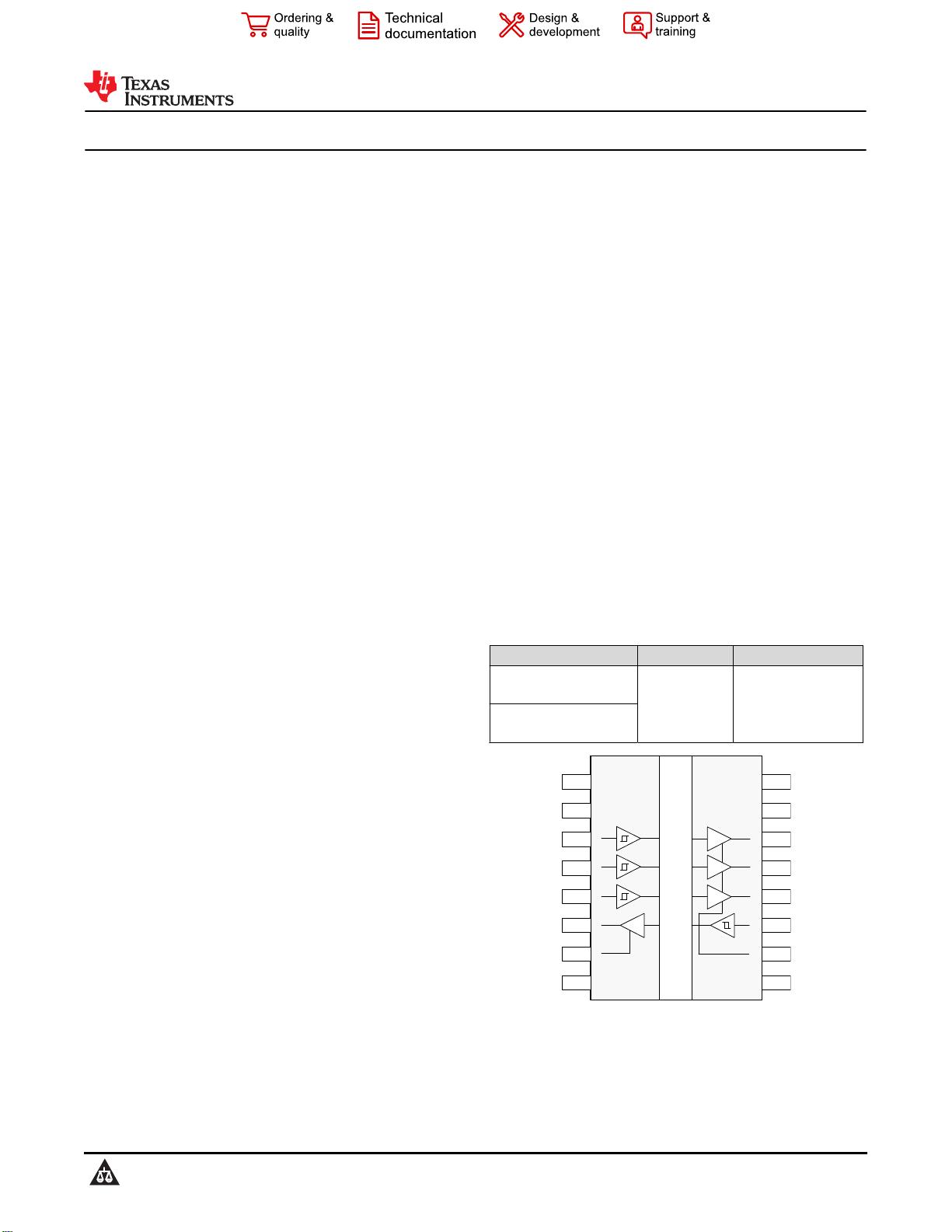
3 Description
The ISOS141-SEP radiation-tolerant device is a high-
performance, quad-channel digital isolator in a small
form factor 16-pin QSOP package. Each isolation
channel has a logic input and output buffer separated
by a double capacitive silicon dioxide (SiO
2
) insulation
barrier. This device supports low Earth orbit (LEO)
space applications with its high data rate of 100
Mbps, low propagation delay of 10.7 ns, and tight
channel-to-channel skew of 4 ns. The ISOS141-SEP
device has three forward and one reverse-direction
channels and if the input power or signal is lost, the
default output is low. The enable pins can be used
to put the respective outputs in high impedance for
multi-master driving applications and to reduce power
consumption.
The ISOS141-SEP provides high electromagnetic
immunity and low emissions with low power
consumption, while isolating CMOS or LVCMOS
digital I/Os. The device has a high common-mode
transient immunity of 100 kV/µs and can ease
system-level ESD, EFT, surge, and simplify emissions
compliance through its innovative chip design.
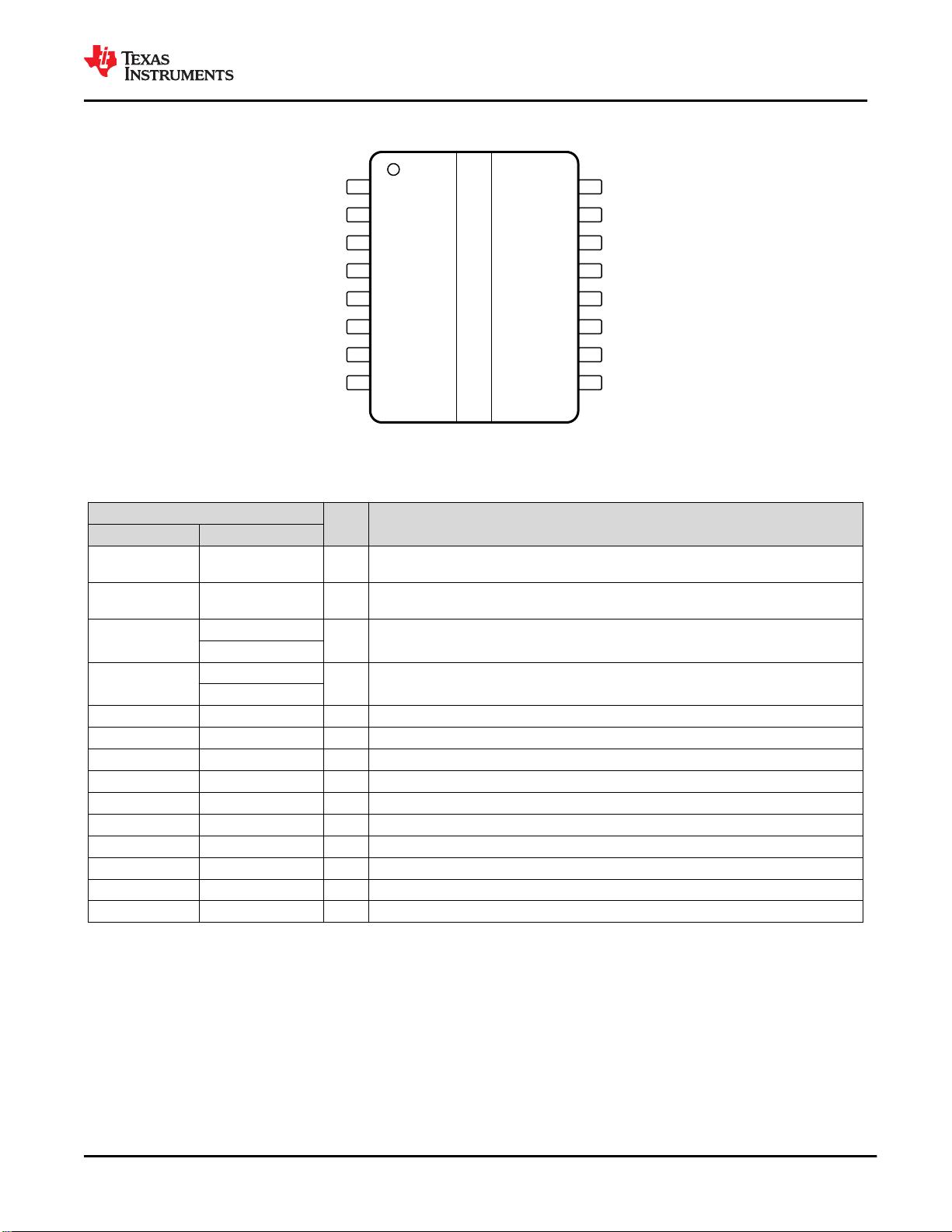
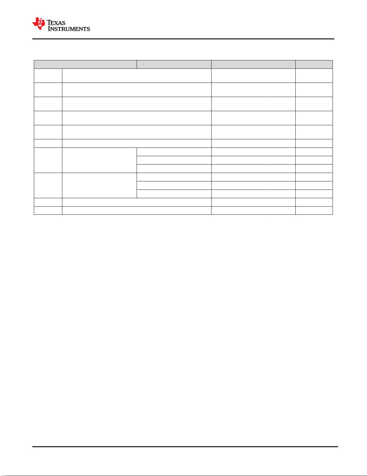
Device Information
PART NUMBER PACKAGE BODY SIZE (NOM)
ISOS141FDBQSEP
30 krad(Si) RLAT/RHA
16-lead
QSOP (DBQ)
4.90 mm × 3.90 mm
ISOS141FDBQTSEP
30 krad(Si) RLAT/RHA
ISOLATION
GND1 GND298
EN1 EN2107
OUTD IND116
INC OUTC125
INB OUTB134
INA OUTA143
GND1 GND2152
V
CC1
V
CC2
161
V
CCI
=Input supply, V
CC2
=Output supply
GND1=Input ground, GND2=Output ground
Simplified Schematic
ISOS141-SEP
SLLSFN1 – MAY 2021
An IMPORTANT NOTICE at the end of this data sheet addresses availability, warranty, changes, use in safety-critical applications,
intellectual property matters and other important disclaimers. PRODUCTION DATA.
Table of Contents
1 Features............................................................................1
2 Applications..................................................................... 1
3 Description.......................................................................1
4 Revision History.............................................................. 2
5 Pin Configuration and Functions...................................3
6 Specifications.................................................................. 4
6.1 Absolute Maximum Ratings ....................................... 4
6.2 ESD Ratings .............................................................. 4
6.3 Recommended Operating Conditions ........................5
6.4 Thermal Information ...................................................6
6.5 Power Ratings ............................................................6
6.6 Insulation Specifications ............................................ 7
6.7 Safety-Related Certifications ..................................... 8
6.8 Safety Limiting Values ................................................8
6.9 Electrical Characteristics—5-V Supply ...................... 9
6.10 Supply Current Characteristics—5-V Supply ........... 9
6.11 Electrical Characteristics—3.3-V Supply ................10
6.12 Supply Current Characteristics—3.3-V Supply ...... 10
6.13 Electrical Characteristics—2.5-V Supply ...............11
6.14 Supply Current Characteristics—2.5-V Supply ...... 11
6.15 Switching Characteristics—5-V Supply ..................12
6.16 Switching Characteristics—3.3-V Supply ...............13
6.17 Switching Characteristics—2.5-V Supply ...............14
6.18 Insulation Characteristics Curves........................... 15
6.19 Typical Characteristics............................................ 16
7 Operating Life Deration.................................................17
8 Parameter Measurement Information.......................... 18
9 Detailed Description......................................................20
9.1 Overview................................................................... 20
9.2 Functional Block Diagram......................................... 20
9.3 Feature Description...................................................21
9.4 Device Functional Modes..........................................22
10 Application and Implementation................................ 23
10.1 Application Information........................................... 23
10.2 Typical Application.................................................. 24
11 Power Supply Recommendations..............................28
12 Layout...........................................................................29
12.1 Layout Guidelines................................................... 29
12.2 Layout Example...................................................... 29
13 Device and Documentation Support..........................30
13.1 Documentation Support.......................................... 30
13.2 Receiving Notification of Documentation Updates..30
13.3 Community Resources............................................30
13.4 Trademarks............................................................. 30
14 Mechanical, Packaging, and Orderable
Information.................................................................... 31
4 Revision History
NOTE: Page numbers for previous revisions may differ from page numbers in the current version.
DATE REVISION NOTES
May 2021 * Initial release.
ISOS141-SEP
SLLSFN1 – MAY 2021
www.ti.com
2 Submit Document Feedback
Copyright © 2021 Texas Instruments Incorporated
Product Folder Links: ISOS141-SEP
5 Pin Configuration and Functions
1VCC1 16 VCC2
2GND1 15 GND2
3INA 14 OUTA
4INB 13 OUTB
5INC 12 OUTC
6OUTD 11 IND
7EN1 10 EN2
8GND1 9 GND2
ISOLATION
Not to scale
Figure 5-1. ISOS141-SEP DBQ Package 16-pin QSOP Top View
Table 5-1. Pin Functions
PIN
I/O DESCRIPTION
NAME Number
EN1 7 I
Output enable 1. Output pins on side 1 are enabled when EN1 is high or open and in
high-impedance state when EN1 is low.
EN2 10 I
Output enable 2. Output pins on side 2 are enabled when EN2 is high or open and in
high-impedance state when EN2 is low.
GND1
2
— Ground connection for V
CC1
8
GND2
9
— Ground connection for V
CC2
15
INA 3 I Input, channel A
INB 4 I Input, channel B
INC 5 I Input, channel C
IND 11 I Input, channel D
OUTA 14 O Output, channel A
OUTB 13 O Output, channel B
OUTC 12 O Output, channel C
OUTD 6 O Output, channel D
V
CC1
1 — Power supply, side 1
V
CC2
16 — Power supply, side 2
www.ti.com
ISOS141-SEP
SLLSFN1 – MAY 2021
Copyright © 2021 Texas Instruments Incorporated
Submit Document Feedback
3
Product Folder Links: ISOS141-SEP
6 Specifications
6.1 Absolute Maximum Ratings
See
(1)
MIN MAX UNIT
Supply voltage
(2)
V
CC1,
V
CC2
-0.5 6 V
Voltage at INx,
OUTx, ENx
V -0.5 V
CCX
+ 0.5
(3)
V
Output current Io -15 15 mA
Temperature
Operating junction temperature, T
J
150 °C
Storage temperature, T
stg
-65 150 °C
(1) Stresses beyond those listed under Absolute Maximum Ratings may cause permanent damage to the device. These are stress
ratings only, which do not imply functional operation of the device at these or any other conditions beyond those indicated under
Recommended Operating Conditions. Exposure to absolute-maximum-rated conditions for extended periods may affect device
reliability.
(2) All voltage values except differential I/O bus voltages are with respect to the local ground terminal (GND1 or GND2) and are peak
voltage values
(3) Maximum voltage must not exceed 6 V.
6.2 ESD Ratings
VALUE UNIT
V
(ESD)
Electrostatic discharge
Human body model (HBM), per ANSI/
ESDA/JEDEC JS-001, all pins
(1)
±6000
V
Charged device model (CDM), per
JEDEC specification JESD22-C101, all
pins
(2)
±1500
Contact discharge per IEC 61000-4-2;
Isolation barrier withstand test
(3)
(4)
±8000
(1) JEDEC document JEP155 states that 500-V HBM allows safe manufacturing with a standard ESD control process.
(2) JEDEC document JEP157 states that 250-V CDM allows safe manufacturing with a standard ESD control process.
(3) IEC ESD strike is applied across the barrier with all pins on each side tied together creating a two-terminal device.
(4) Testing is carried out in air or oil to determine the intrinsic contact discharge capability of the device.
ISOS141-SEP
SLLSFN1 – MAY 2021
www.ti.com
4 Submit Document Feedback
Copyright © 2021 Texas Instruments Incorporated
Product Folder Links: ISOS141-SEP
6.3 Recommended Operating Conditions
over operating free-air temperature range (unless otherwise noted)
MIN NOM MAX UNIT
V
CC1 ,
V
CC2
(1)
Supply Voltage 2.25 5.5 V
Vcc
(UVLO+)
UVLO threshold when supply voltage is rising 2 2.25 V
Vcc
(UVLO-)
UVLO threshold when supply voltage is falling 1.7 1.8 V
Vhys
(UVLO)
Supply voltage UVLO hysteresis 100 200 mV
V
IH
High level Input voltage
0.7 x V
CCI
(2)
V
CCI
V
V
IL
Low level Input voltage 0 0.3 x V
CCI
V
I
OH
High level output current
V
CCO
= 5 V
(2)
-4 mA
V
CCO
= 3.3 V -2 mA
V
CCO
= 2.5 V -1 mA
I
OL
Low level output current
V
CCO
= 5 V 4 mA
V
CCO
= 3.3 V 2 mA
V
CCO
= 2.5 V 1 mA
DR Data Rate 0 100 Mbps
T
A
Ambient temperature -55 25 125 °C
(1) V
CC1
and V
CC2
can be set independent of one another
(2) V
CCI
= Input-side V
CC
; V
CCO
= Output-side V
CC
www.ti.com
ISOS141-SEP
SLLSFN1 – MAY 2021
Copyright © 2021 Texas Instruments Incorporated
Submit Document Feedback
5
Product Folder Links: ISOS141-SEP
剩余39页未读,继续阅读
资源评论
不觉明了
- 粉丝: 3101
- 资源: 5337
上传资源 快速赚钱
- 我的内容管理 展开
- 我的资源 快来上传第一个资源
- 我的收益 登录查看自己的收益
- 我的积分 登录查看自己的积分
- 我的C币 登录后查看C币余额
- 我的收藏
- 我的下载
- 下载帮助
安全验证
文档复制为VIP权益,开通VIP直接复制
信息提交成功