TI-LF298.pdf
需积分: 9 107 浏览量
2022-11-25
23:48:56
上传
评论 5
收藏 2.87MB PDF 举报

Product
Folder
Sample &
Buy
Technical
Documents
Tools &
Software
Support &
Community
LF198-N
,
LF298
,
LF398-N
LF198A-N
,
LF398A-N
SNOSBI3B –JULY 2000–REVISED NOVEMBER 2015
LF298, LFx98x Monolithic Sample-and-Hold Circuits
1 Features 3 Description
The LF298 and LFx98x devices are monolithic
1
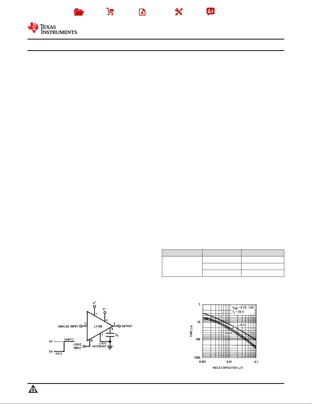
• Operates from ±5-V to ±18-V Supplies
sample-and-hold circuits that use BI-FET technology
• Less than 10-μs Acquisition Time
to obtain ultrahigh DC accuracy with fast acquisition
• Logic Input Compatible With TTL, PMOS, CMOS
of signal and low droop rate. Operating as a unity-
gain follower, DC gain accuracy is 0.002% typical and
• 0.5-mV Typical Hold Step at Ch = 0.01 µF
acquisition time is as low as 6 µs to 0.01%. A bipolar
• Low Input Offset
input stage is used to achieve low offset voltage and
• 0.002% Gain Accuracy
wide bandwidth. Input offset adjust is accomplished
with a single pin and does not degrade input offset
• Low Output Noise in Hold Mode
drift. The wide bandwidth allows the LF198-N to be
• Input Characteristics Do Not Change During Hold
included inside the feedback loop of 1-MHz
Mode
operational amplifiers without having stability
• High Supply Rejection Ratio in Sample or Hold
problems. Input impedance of 10
10
Ω allows high-
• Wide Bandwidth
source impedances to be used without degrading
accuracy.
• Space Qualified, JM38510
P-channel junction FETs are combined with bipolar
2 Applications
devices in the output amplifier to give droop rates as
low as 5 mV/min with a 1-µF hold capacitor. The
• Ramp Generators With Variable Reset Level
JFETs have much lower noise than MOS devices
• Integrators With Programmable Reset Level
used in previous designs and do not exhibit high
• Synchronous Correlators
temperature instabilities. The overall design ensures
no feedthrough from input to output in the hold mode,
• 2-Channel Switches
even for input signals equal to the supply voltages.
• DC and AC Zeroing
Logic inputs on the LF198-N are fully differential with
• Staircase Generators
low input current, allowing for direct connection to
TTL, PMOS, and CMOS. Differential threshold is
1.4 V. The LF198-N will operate from ±5-V to ±18-V
supplies.
An A version is available with tightened electrical
specifications.
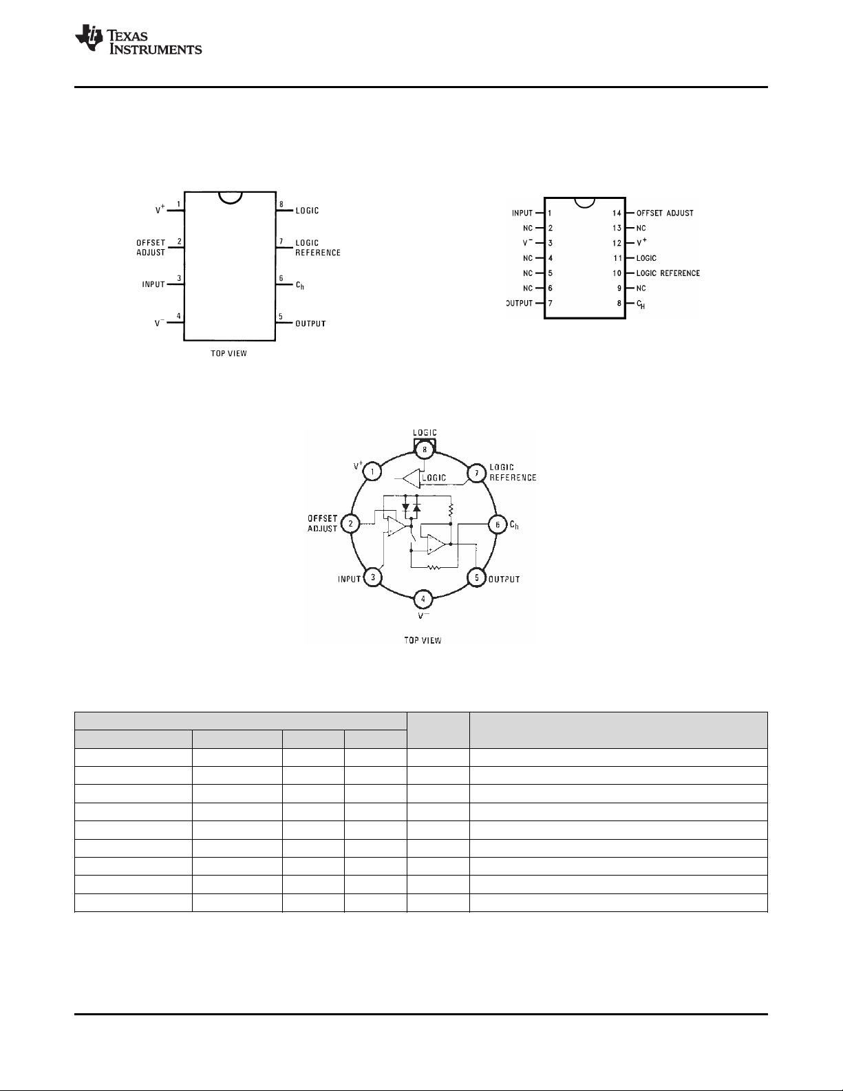
Device Information
(1)
PART NUMBER PACKAGE BODY SIZE (NOM)
SOIC (14) 8.65 mm × 3.91 mm
LF298, LFx98x TO-99 (8) 9.08 mm × 9.08 mm
PDIP (8) 9.81 mm × 6.35 mm
(1) For all available packages, see the orderable addendum at
the end of the data sheet.
Typical Connection
Acquisition Time
1
An IMPORTANT NOTICE at the end of this data sheet addresses availability, warranty, changes, use in safety-critical applications,
intellectual property matters and other important disclaimers. PRODUCTION DATA.

剩余32页未读,继续阅读


评论0
最新资源