没有合适的资源?快使用搜索试试~ 我知道了~
DIODES-AP62301.pdf
需积分: 8 0 下载量 75 浏览量
2022-10-22
13:44:08
上传
评论 5
收藏 1.78MB PDF 举报
温馨提示
试读
24页
DIODES-AP62301.pdf
资源详情
资源评论
资源推荐
AP62300/AP62301/AP62300T
Document number: DS41958 Rev. 2 - 2
1 of 24
www.diodes.com
May 2020
© Diodes Incorporated
AP62300/AP62301/AP62300T
4.2V TO 18V INPUT, 3A LOW IQ SYNCHRONOUS BUCK CONVERTER
Description
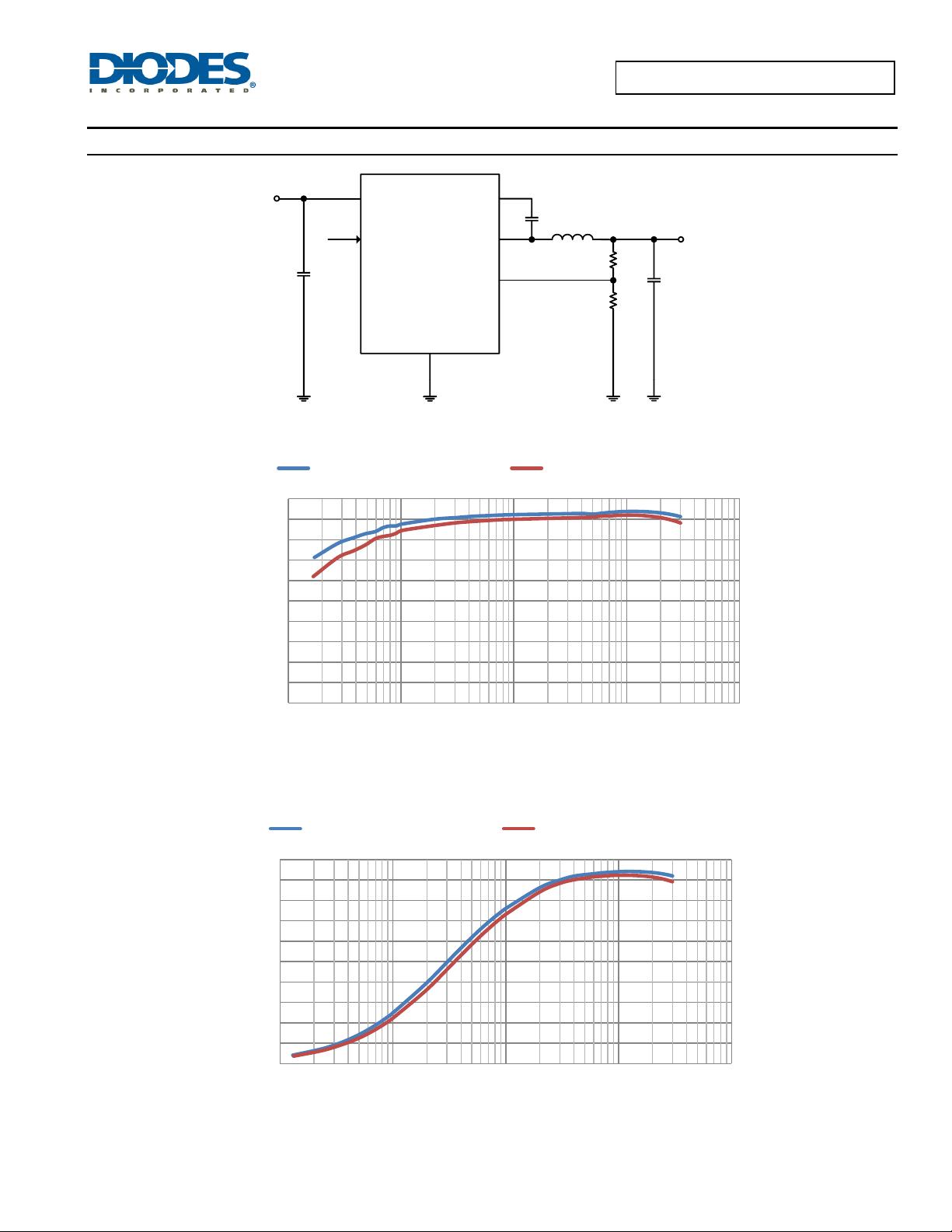
The AP62300/AP62301/AP62300T is a 3A, synchronous buck
converter with a wide input voltage range of 4.2V to 18V. The device
fully integrates a 75mΩ high-side power MOSFET and a 45mΩ low-
side power MOSFET to provide high-efficiency step-down DC-DC
conversion.
The AP62300/AP62301/AP62300T device is easily used by
minimizing the external component count due to its adoption of
Constant On-Time (COT) control to achieve fast transient response,
easy loop stabilization, and low output voltage ripple.
The AP62300/AP62301/AP62300T design is optimized for
Electromagnetic Interference (EMI) reduction. The device has a
proprietary gate driver scheme to resist switching node ringing without
sacrificing MOSFET turn-on and turn-off times, which reduces high-
frequency radiated EMI noise caused by MOSFET switching.
AP62300/AP62301 is available in SOT563 and TSOT26 packages.
AP62300T is available in a TSOT26 package.
Features
VIN: 4.2V to 18V
Output Voltage (VOUT): 0.8V to 7V
3A Continuous Output Current
0.8V ± 1% Reference Voltage (T
A
= +25°C)
AP62300 and AP62301
0.763V ± 1% Reference Voltage (T
A
= +25°C)
AP62300T
155μA Low Quiescent Current (Pulse Frequency Modulation)
750kHz Switching Frequency (VIN = 12V, VOUT = 5V)
Up to 83% Efficiency at 5mA Light Load
Proprietary Gate Driver Design for Best EMI Reduction
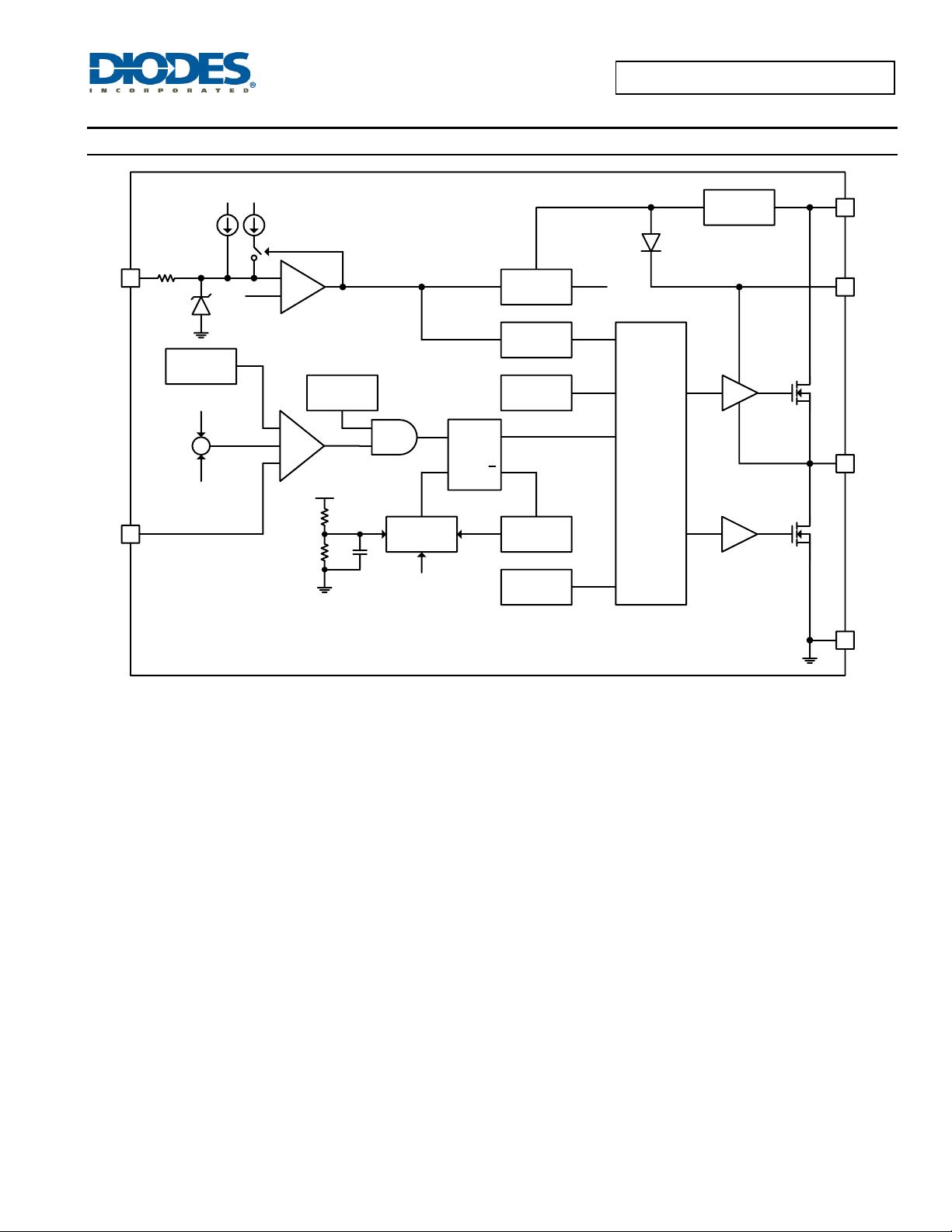
Protection Circuitry
Undervoltage Lockout (UVLO)
Cycle-by-Cycle Valley Current Limit
Thermal Shutdown
Totally Lead-Free & Fully RoHS Compliant (Notes 1 & 2)
Halogen and Antimony Free. “Green” Device (Note 3)
For automotive applications requiring specific change
control (i.e. parts qualified to AEC-Q100/101/200, PPAP
capable, and manufactured in IATF 16949 certified facilities),
please contact us or your local Diodes representative.
https://www.diodes.com/quality/product-definitions/
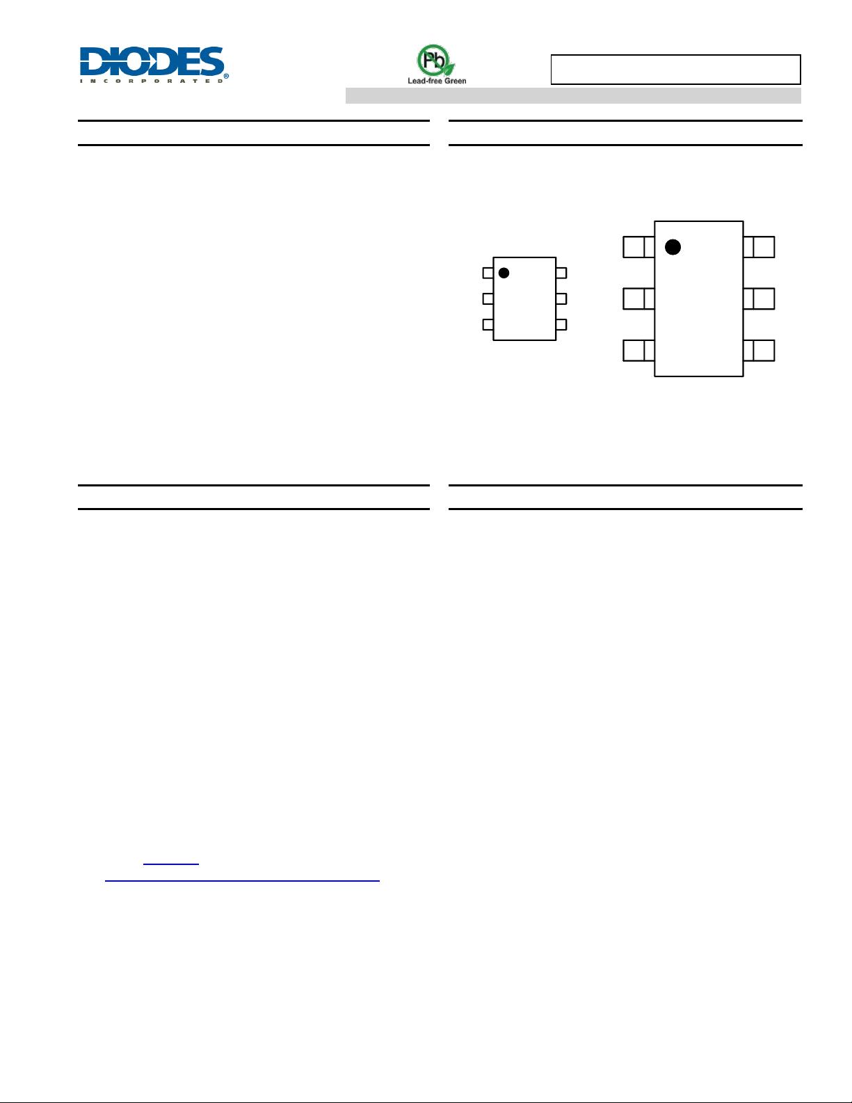
Pin Assignments
1
2
3 4
5
6GND
SW
VIN FB
EN
BST
TSOT26
(Top View)
1
2
3 4
5
6 FB
EN
BSTGND
SW
VIN
SOT563
(Top View)
Applications
5V and 12V Distributed Power Bus Supplies
Flat Screen TV Sets and Monitors
White Goods and Small Home Appliances
FPGA, DSP, and ASIC Supplies
Home Audio
Network Systems
Gaming Consoles
Consumer Electronics
General Purpose Point of Load
Notes: 1. No purposely added lead. Fully EU Directive 2002/95/EC (RoHS), 2011/65/EU (RoHS 2) & 2015/863/EU (RoHS 3) compliant.
2. See https://www.diodes.com/quality/lead-free/ for more information about Diodes Incorporated’s definitions of Halogen- and Antimony-free, "Green" and
Lead-free.
3. Halogen- and Antimony-free "Green” products are defined as those which contain <900ppm bromine, <900ppm chlorine (<1500ppm total Br + Cl) and
<1000ppm antimony compounds.
AP62300/AP62301/AP62300T
Document number: DS41958 Rev. 2 - 2
2 of 24
www.diodes.com
May 2020
© Diodes Incorporated
AP62300/AP62301/AP62300T
Typical Application Circuit
AP62300
AP62301
AP62300T
VIN
EN SW
BST
FB
GND
INPUT
R1
R2
L
3.3μH
C3
100nF
C2
2 x 22µF
C1
10µF
OUTPUT
VOUT
5V
Figure 1. Typical Application Circuit
Figure 2. Efficiency vs. Output Current, AP62300/AP62300T
Figure 3. Efficiency vs. Output Current, AP62301
0
10
20
30
40
50
60
70
80
90
100
0.001 0.010 0.100 1.000 10.000
Efficiency (%)
IOUT (A)
VIN = 12V, VOUT = 5V, L = 3.3μH VIN = 12V, VOUT = 3.3V, L = 3.3μH
0
10
20
30
40
50
60
70
80
90
100
0.001 0.010 0.100 1.000 10.000
Efficiency (%)
IOUT (A)
VIN = 12V, VOUT = 5V, L = 3.3μH VIN = 12V, VOUT = 3.3V, L = 3.3μH
AP62300/AP62301/AP62300T
Document number: DS41958 Rev. 2 - 2
3 of 24
www.diodes.com
May 2020
© Diodes Incorporated
AP62300/AP62301/AP62300T
Pin Descriptions
Pin
Name
Pin Number
Function
SOT563
TSOT26
VIN
1
3
Power Input. VIN supplies the power to the IC as well as the step-down converter power MOSFETs. Drive VIN with
a 4.2V to 18V power source. Bypass VIN to GND with a suitably large capacitor to eliminate noise due to the
switching of the IC. See Input Capacitor section for more details.
SW
2
2
Power Switching Output. SW is the switching node that supplies power to the output. Connect the output LC filter
from SW to the output load.
GND
3
1
Power Ground.
BST
4
6
High-Side Gate Drive Boost Input. BST supplies the drive for the high-side N-Channel MOSFET. A 100nF
capacitor is recommended from BST to SW to power the high-side driver.
EN
5
5
Enable Input. EN is a digital input that turns the regulator on or off. Drive EN high to turn on the regulator and low
to turn it off. Leave floating for automatic startup. The EN has a precision threshold of 1.2V for programing the
UVLO. See Enable section for more details.
FB
6
4
Feedback sensing terminal for the output voltage. Connect this pin to the resistive divider of the output. See
Setting the Output Voltage section for more details.
AP62300/AP62301/AP62300T
Document number: DS41958 Rev. 2 - 2
4 of 24
www.diodes.com
May 2020
© Diodes Incorporated
AP62300/AP62301/AP62300T
Functional Block Diagram
EN
FB
SW
VIN
VREF
VCC
BST
GND
+
+
-
+
Control
Logic
S
E
Thermal
Shutdown
S
VIN
Q
R
Q
SW
On-Time
Compute
One-Shot
Minimum
Off-Time
OCP
UVLO
Internal
Reference
Internal
Soft-Start
VREF
VCC
Regulator
BST
Q1
Q2
ON
1.2V
I1
1.5μA
20kΩ
+
–
I2
5.5μA
Figure 4. Functional Block Diagram
AP62300/AP62301/AP62300T
Document number: DS41958 Rev. 2 - 2
5 of 24
www.diodes.com
May 2020
© Diodes Incorporated
AP62300/AP62301/AP62300T
Absolute Maximum Ratings (Note 4) (@ T
A
= +25°C, unless otherwise specified.)
Symbol
Parameter
Rating
Unit
VIN
Supply Pin Voltage
-0.3 to +20.0 (DC)
V
-0.3 to +22.0 (400ms)
V
SW
Switch Pin Voltage
-1.0 to VIN + 0.3 (DC)
V
-2.5 to VIN + 2.0 (20ns)
V
BST
Bootstrap Pin Voltage
V
SW
- 0.3 to V
SW
+ 6.0
V
V
EN
Enable/UVLO Pin Voltage
-0.3 to +6.0
V
V
FB
Feedback Pin Voltage
-0.3 to +6.0
V
T
ST
Storage Temperature
-65 to +150
°C
T
J
Junction Temperature
+160
°C
T
L
Lead Temperature
+260
°C
ESD Susceptibility (Note 5)
HBM
Human Body Model
±2000
V
CDM
Charged Device Model
±500
V
Notes: 4. Stresses greater than the Absolute Maximum Ratings specified above can cause permanent damage to the device. These are stress ratings only;
functional operation of the device at these or any other conditions exceeding those indicated in this specification is not implied. Device reliability can
be affected by exposure to absolute maximum rating conditions for extended periods of time.
5. Semiconductor devices are ESD sensitive and can be damaged by exposure to ESD events. Suitable ESD precautions should be taken when
handling and transporting these devices.
Thermal Resistance (Note 6)
Symbol
Parameter
Rating
Unit
θ
JA
Junction to Ambient
SOT563
110
°C/W
TSOT26
70
θ
JC
Junction to Case
SOT563
8
°C/W
TSOT26
12
Note: 6. Test condition for SOT563/TSOT26: Device mounted on FR-4 substrate, two-layer PCB, 2oz copper, with minimum recommended pad layout.
Recommended Operating Conditions (Note 7) (@ T
A
= +25°C, unless otherwise specified.)
Symbol
Parameter
Min
Max
Unit
VIN
Supply Voltage
4.2
18.0
V
VOUT
Output Voltage
0.8
7.0
V
T
A
Operating Ambient Temperature
-40
+85
°C
T
J
Operating Junction Temperature
-40
+125
°C
Note: 7. The device function is not guaranteed outside of the recommended operating conditions.
剩余23页未读,继续阅读
不觉明了
- 粉丝: 3175
- 资源: 5430
上传资源 快速赚钱
- 我的内容管理 展开
- 我的资源 快来上传第一个资源
- 我的收益 登录查看自己的收益
- 我的积分 登录查看自己的积分
- 我的C币 登录后查看C币余额
- 我的收藏
- 我的下载
- 下载帮助
安全验证
文档复制为VIP权益,开通VIP直接复制
信息提交成功
评论0