System Description
www.ti.com
1 System Description
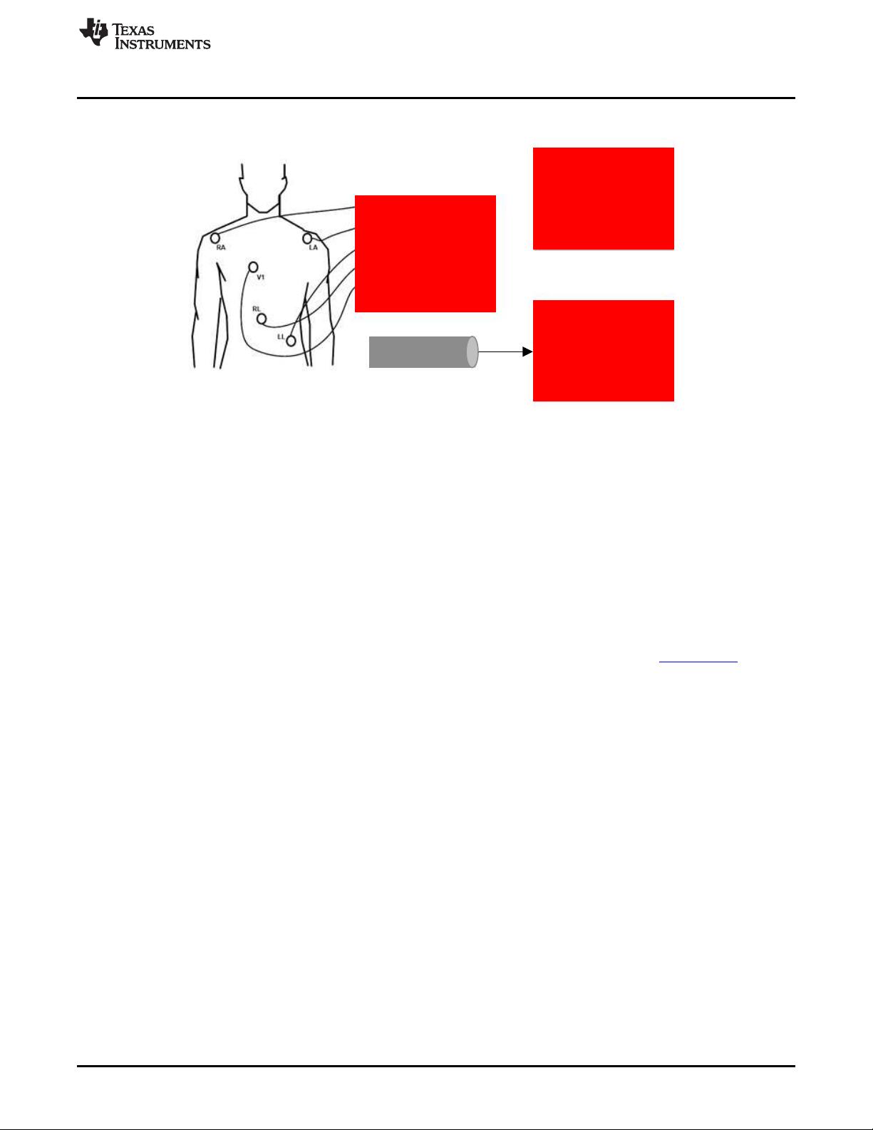
The heart of the Wireless Heart Rate Monitor is the ADS1293 device (analog front-end) and the CC2541
device (Bluetooth-low energy SOC) as shown in Figure 1. The ADS1293 device is a highly integrated low-
power analog front-end (AFE) that features three high-resolution ECG channels. The CC2541 system-on-
chip (SoC) adds a BLE wireless feature to the platform. BLE enables seamless connectivity to an iPhone®
or an iPad® through a configurable iOS application that allows an end-user to remotely monitor the heart-
rate data of a patient.
1.1 ADS1293
The ADS1293 incorporates all features commonly required in portable, low-power medical, sports, and
fitness electrocardiogram (ECG) applications. With high levels of integration and exceptional performance,
the ADS1293 enables the creation of scalable medical instrumentation systems at significantly reduced
size, power, and overall cost.
The ADS1293 features three high-resolution channels capable of operating up to 25.6ksps. Each channel
can be independently programmed for a specific sample rate and bandwidth allowing users to optimize the
configuration for performance and power. All input pins incorporate an EMI filter and can be routed to any
channel via a flexible routing switch. Flexible routing also allows independent lead-off detection, right leg
drive, and Wilson/Goldberger reference terminal generation without the need to reconnect leads
externally. A fourth channel allows external analog pace detection for applications that do not utilize digital
pace detection. For the ADS1293 block diagram, see Figure 2.
The ADS1293 incorporates a self-diagnostics alarm system to detect when the system is out of the
operating conditions range. Such events are reported to error flags. The overall status of the error flags is
available as a signal on a dedicated ALARMB pin. The device is packaged in a 5-mm × 5-mm × 0,8-mm,
28-pin LLP. Operating temperature ranges from –20°C to 85°C.
1.2 CC2541
The CC2541 is a power-optimized true system-on-chip (SoC) solution for both Bluetooth low energy and
proprietary 2.4-GHz applications. It enables robust network nodes to be built with low total bill-of-material
costs. The CC2541 combines the excellent performance of a leading RF transceiver with an industry-
standard enhanced 8051 MCU, in-system programmable flash memory, 8-KB RAM, and many other
powerful supporting features and peripherals. The CC2541 is highly suited for systems where ultralow
power consumption is required. This is specified by various operating modes. Short transition times
between operating modes further enable low power consumption.
The CC2541 is pin-compatible with the CC2540 in the 6-mm × 6-mm QFN40 package, if the USB is not
used on the CC2540 and the I
2
C/extra I/O is not used on the CC2541. Compared to the CC2540, the
CC2541 provides lower RF current consumption. The CC2541 does not have the USB interface of the
CC2540, and provides lower maximum output power in TX mode. The CC2541 also adds a HW I
2
C
interface.
The CC2541 is pin-compatible with the CC2533 RF4CE-optimized IEEE 802.15.4 SoC. The CC2541
comes in two different versions: CC2541F128/F256, with 128 KB and 256 KB of flash memory,
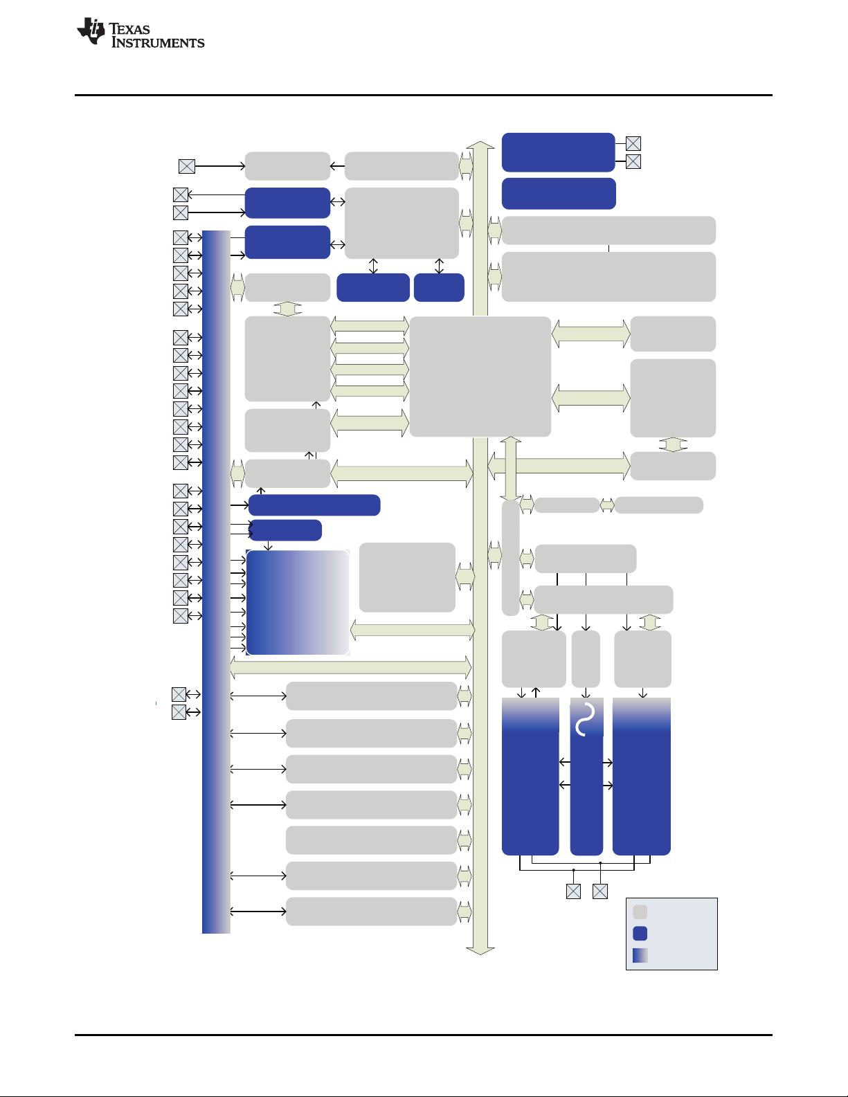
respectively. For the CC2541 block diagram, see Figure 3.
1.3 TPS61220
The TPS6122x family devices provide a power-supply solution for products powered by either a single-
cell, two-cell, or three-cell alkaline, NiCd or NiMH, or one-cell Li-Ion or Li-polymer battery. Possible output
currents depend on the input-to-output voltage ratio. The boost converter is based on a hysteretic
controller topology using synchronous rectification to obtain maximum efficiency at minimal quiescent
currents. The output voltage of the adjustable version can be programmed by an external resistor divider,
or is set internally to a fixed output voltage. The converter can be switched off by a featured enable pin.
While being switched off, battery drain is minimized. The device is offered in a 6-pin SC-70 package
(DCK) measuring 2 mm × 2 mm to enable small circuit layout size. For the TPS61220 block diagram, see
Figure 4.
2
Wireless Heart Rate Monitor Reference Design TIDU195A–January 2014–Revised July 2014
Submit Documentation Feedback
Copyright © 2014, Texas Instruments Incorporated


