ADS8674/ADS8678数据手册
需积分: 0 70 浏览量
2024-01-08
16:05:42
上传
评论
收藏 3.42MB PDF 举报

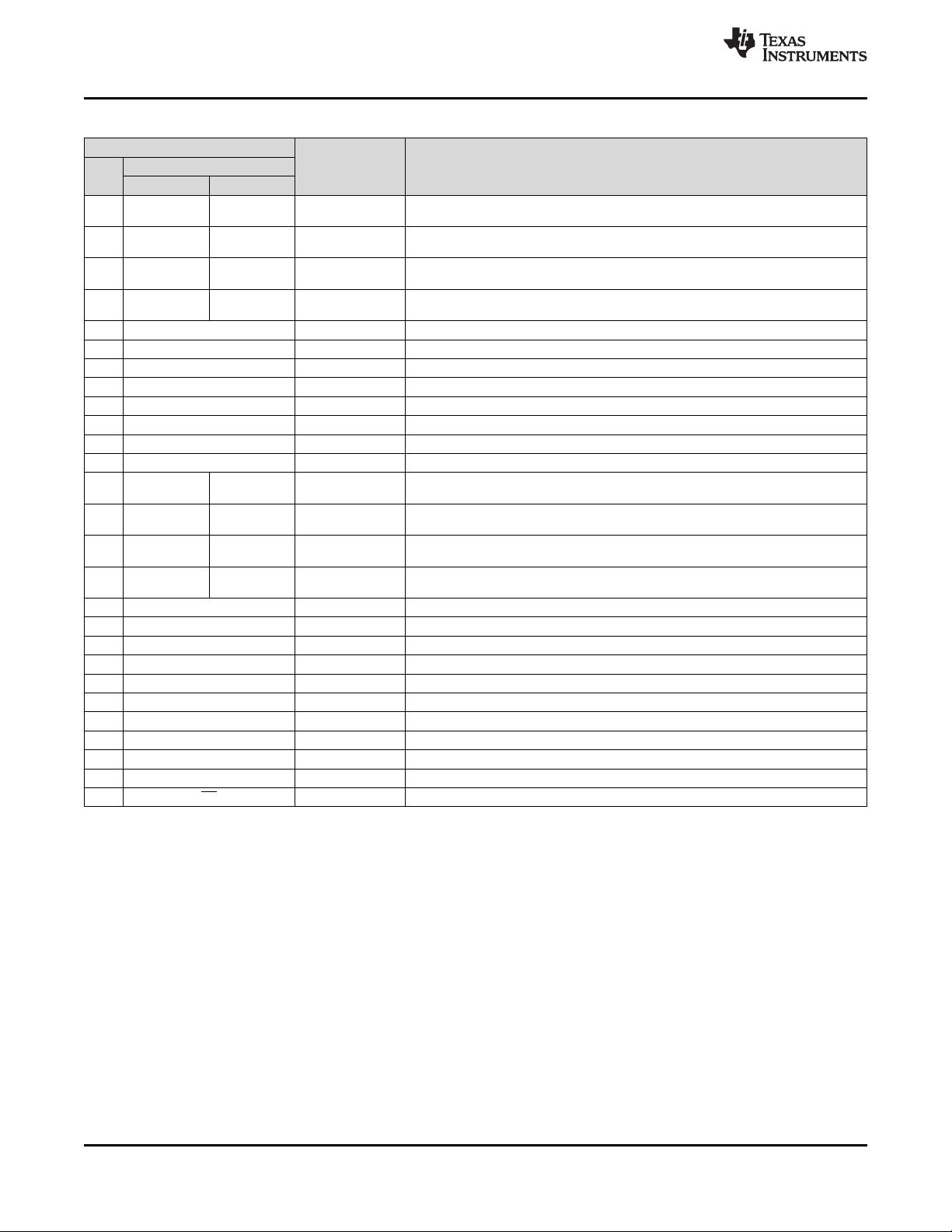
-0.05
-0.03
-0.01
0.01
0.03
0.05
±40 ±7
26 59 92 125
Gain (% FS)
Free-Air Temperature (
o
C)
C039
---- ± 2.5*V
REF,
---- 1.25*V
REF
---- 0.625*V
REF,
------0.3125*V
REF
-------0.156 V
REF,
---- + 2.5*V
REF
---- + 1.25*V
REF,
---- + 0.625*V
REF
---- + 0.3125*V
REF
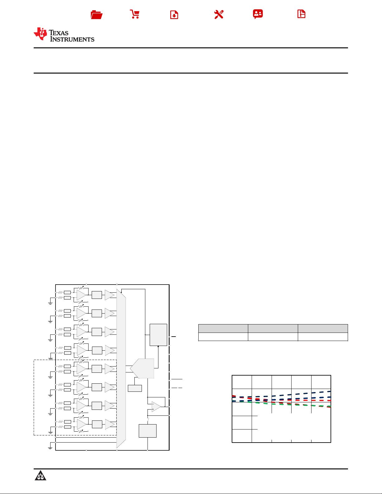
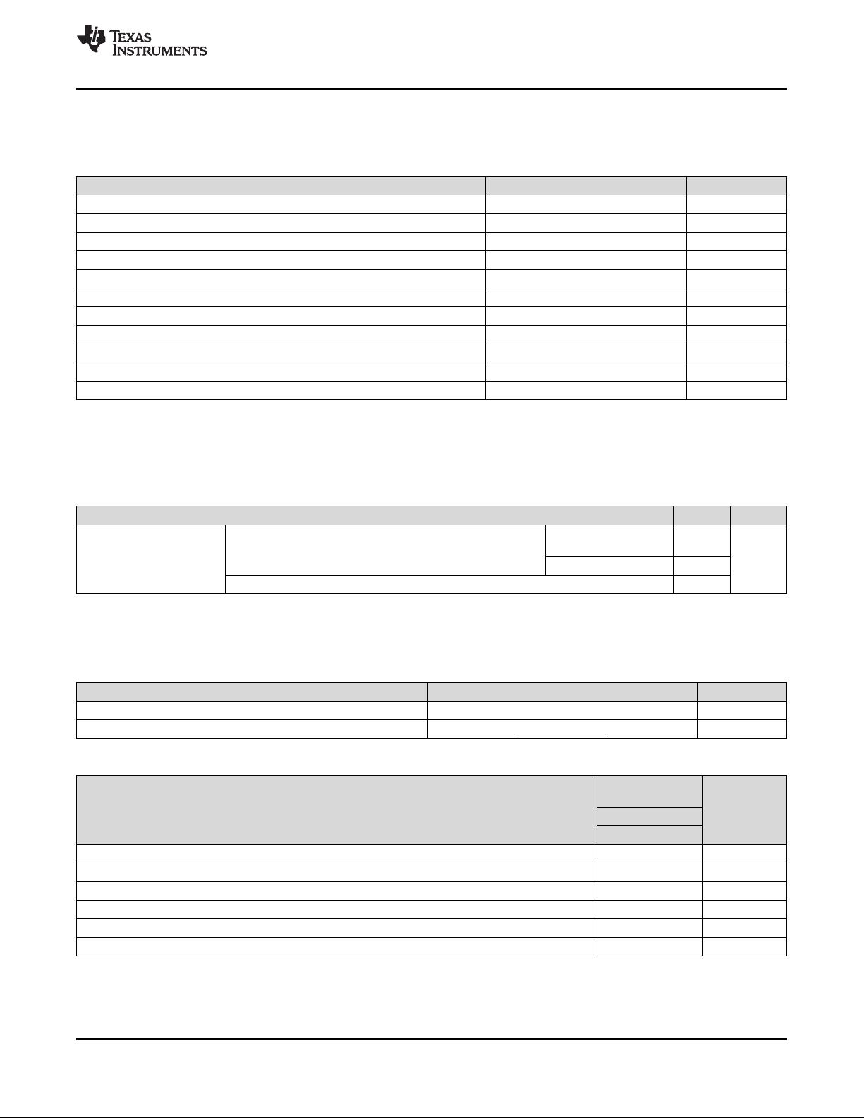
Multiplexer
Oscillator
CS
SCLK
SDI
SDO
DAISY
REFSEL
RST/PD
REFCAP
REFIO
PGA
1 M:
OVP
1 M:
2nd-Order
LPF
ADC
Driver
V
B0
AIN_0P
AIN_0GND
OVP
PGA
1 M:
OVP
1 M:
2nd-Order
LPF
ADC
Driver
V
B1
AIN_1P
AIN_1GND
OVP
PGA
1 M:
OVP
1 M:
2nd-Order
LPF
ADC
Driver
V
B2
AIN_2P
AIN_2GND
OVP
PGA
1 M:
OVP
1 M:
2nd-Order
LPF
ADC
Driver
V
B3
AIN_3P
AIN_3GND
OVP
PGA
1 M:
OVP
1 M:
2nd-Order
LPF
ADC
Driver
V
B4
AIN_4P
AIN_4GND
OVP
PGA
1 M:
OVP
1 M:
2nd-Order
LPF
ADC
Driver
V
B5
AIN_5P
AIN_5GND
OVP
PGA
1 M:
OVP
1 M:
2nd-Order
LPF
ADC
Driver
V
B6
AIN_6P
AIN_6GND
OVP
PGA
1 M:
OVP
1 M:
2nd-Order
LPF
ADC
Driver
V
B7
AIN_7P
AIN_7GND
OVP
AUX_IN
AUX_GND
14-Bit
SAR ADC
Digital
Logic
and
Interface
4.096-V
Reference
REFGND
DGNDAGND
DVDD
AVDD
Additional Channels in ADS8678
ADS8678
ADS8674
ALARM
Product
Folder
Sample &
Buy
Technical
Documents
Tools &
Software
Support &
Community
Reference
Design
ADS8674
,
ADS8678
SBAS627 –JULY 2015
ADS867x 14-Bit, 500-kSPS, 4- and 8-Channel, Single-Supply, SAR ADCs with
Bipolar Input Ranges
1 Features 2 Applications
1
• 14-Bit ADCs with Integrated Analog Front-End
• Power Automation
• 4-, 8-Channel MUX with Auto and Manual Scan • Protection Relays
• Channel-Independent Programmable Inputs: • PLC Analog Input Modules
– ±10.24 V, ±5.12 V, ±2.56 V, ±1.28 V, ±0.64 V
3 Description
– 10.24 V, 5.12 V, 2.56 V, 1.28 V
The ADS8674 and ADS8678 are 4- and 8-channel,
• 5-V Analog Supply: 1.65-V to 5-V I/O Supply
integrated data acquisition systems based on a 14-bit
• Constant Resistive Input Impedance: 1 MΩ
successive approximation (SAR) analog-to-digital
converter (ADC), operating at a throughput of
• Input Overvoltage Protection: Up to ±20 V
500 kSPS. The devices feature integrated analog
• On-Chip, 4.096-V Reference with Low Drift
front-end circuitry for each input channel with
• Excellent Performance:
overvoltage protection up to ±20 V, a 4- or 8-channel
multiplexer with automatic and manual scanning
– 500-kSPS Aggregate Throughput
modes, and an on-chip, 4.096-V reference with low
– DNL: ±0.2 LSB; INL: ±0.25 LSB
temperature drift. Operating on a single 5-V analog
– Low Drift for Gain Error and Offset
supply, each input channel on the devices can
– SNR: 85 dB; THD: –100 dB
support true bipolar input ranges of ±10.24 V,
±5.12 V, ±2.56 V, ±1.28V and ±0.64V, as well as
– Low Power: 65 mW
unipolar input ranges of 0 V to 10.24 V, 0 V to 5.12 V,
• AUX Input → Direct Connection to ADC Inputs
0 V to 2.56 V and 0 V to 1.28 V. The gain of the
• ALARM → High and Low Thresholds per Channel
analog front-end for all input ranges is accurately
trimmed to ensure a high dc precision. The input
• SPI™-Compatible Interface with Daisy-Chain
range selection is software-programmable and
• Industrial Temperature Range: –40°C to 125°C
independent for each channel. The devices offer a
• TSSOP-38 Package (9.7 mm × 4.4 mm)
1-MΩ constant resistive input impedance irrespective
of the selected input range.
Block Diagram
The ADS8674 and ADS8678 offer a simple SPI-
compatible serial interface to the digital host and also
support daisy-chaining of multiple devices. The digital
supply operates from 1.65 V to 5.25 V, enabling
direct interface to a wide range of host controllers.
Device Information
(1)
PART NUMBER PACKAGE BODY SIZE (NOM)
ADS867x TSSOP (38) 9.70 mm × 4.40 mm
(1) For all available packages, see the orderable addendum at
the end of the datasheet.
Gain Error versus Temperature
1
An IMPORTANT NOTICE at the end of this data sheet addresses availability, warranty, changes, use in safety-critical applications,
intellectual property matters and other important disclaimers. PRODUCTION DATA.
剩余78页未读,继续阅读
资源评论


