DAC128S085.pdf
需积分: 48 85 浏览量
2020-12-22
10:15:46
上传
评论
收藏 526KB PDF 举报

September 2007
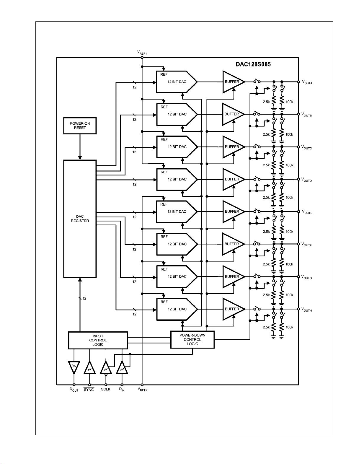
DAC128S085
12-Bit Micro Power OCTAL Digital-to-Analog Converter
with Rail-to-Rail Outputs
General Description
The DAC128S085 is a full-featured, general purpose OCTAL
12-bit voltage-output digital-to-analog converter (DAC) that
can operate from a single +2.7V to +5.5V supply and con-
sumes 1.95 mW at 3V and 4.85 mW at 5V. The DAC128S085
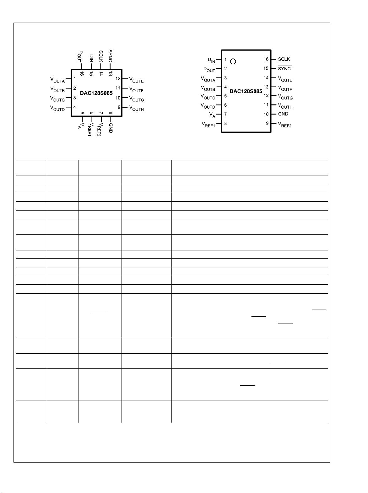
is packaged in a 16-lead LLP package and a 16-lead TSSOP
package. The LLP package makes the DAC128S085 the
smallest OCTAL DAC in its class. The on-chip output ampli-
fiers allow rail-to-rail output swing and the three wire serial
interface operates at clock rates up to 40 MHz over the entire
supply voltage range. Competitive devices are limited to 25
MHz clock rates at supply voltages in the 2.7V to 3.6V range.
The serial interface is compatible with standard SPI™, QSPI,
MICROWIRE and DSP interfaces. The DAC128S085 also of-
fers daisy chain operation where an unlimited number of
DAC128S085s can be updated simultaneously using a single
serial interface.
There are two references for the DAC128S085. One refer-
ence input serves channels A through D while the other
reference serves channels E through H. Each reference can
be set independently between 0.5V and V
A
, providing the
widest possible output dynamic range. The DAC128S085 has
a 16-bit input shift register that controls the mode of operation,
the power-down condition, and the DAC channels' register/
output value. All eight DAC outputs can be updated simulta-
neously or individually.
A power-on reset circuit ensures that the DAC outputs power
up to zero volts and remain there until there is a valid write to
the device. The power-down feature of the DAC128S085 al-
lows each DAC to be independently powered with three dif-
ferent termination options. With all the DAC channels
powered down, power consumption reduces to less than 0.3
µW at 3V and less than 1 µW at 5V. The low power consump-
tion and small packages of the DAC128S085 make it an
excellent choice for use in battery operated equipment.
The DAC128S085 is one of a family of pin compatible DACs,
including the 8-bit DAC088S085 and the 10-bit DAC108S085.
All three parts are offered with the same pinout, allowing sys-
tem designers to select a resolution appropriate for their
application without redesigning their printed circuit board. The
DAC128S085 operates over the extended industrial temper-
ature range of −40°C to +125°C.
Features
■
Guaranteed Monotonicity
■
Low Power Operation
■
Rail-to-Rail Voltage Output
■
Daisy Chain Capability
■
Power-on Reset to 0V
■
Simultaneous Output Updating
■
Individual Channel Power Down Capability
■
Wide power supply range (+2.7V to +5.5V)
■
Dual Reference Voltages with range of 0.5V to V
A
■
Operating Temperature Range of −40°C to +125°C
■
Industry's Smallest Package
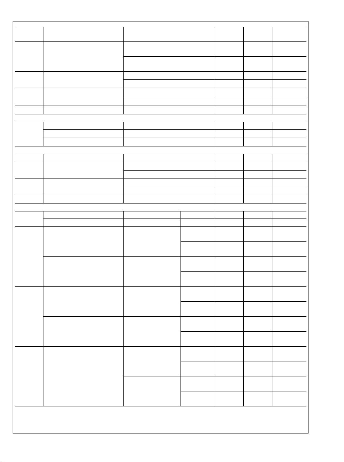
Key Specifications
■
Resolution 12 bits
■
INL ±8 LSB (max)
■
DNL +0.75 / −0.4 LSB (max)
■
Settling Time 8.5 µs (max)
■
Zero Code Error +15 mV (max)
■
Full-Scale Error −0.75 %FSR (max)
■
Supply Power
■
—
Normal 1.95 mW (3V) / 4.85 mW (5V) typ
—
Power Down 0.3 µW (3V) / 1 µW (5V) typ
Applications
■
Battery-Powered Instruments
■
Digital Gain and Offset Adjustment
■
Programmable Voltage & Current Sources
■
Programmable Attenuators
■
Voltage Reference for ADCs
■
Sensor Supply Voltage
■
Range Detectors
Ordering Information
Order Numbers Temperature Range Package Top Mark
DAC128S085CISQ
−40°C ≤ T
A
≤ +125°C
16-Lead LLP
DAC128S085CISQX
−40°C ≤ T
A
≤ +125°C
LLP Tape-and-Reel
DAC128S085CIMT
−40°C ≤ T
A
≤ +125°C
16-Lead TSSOP X78C
DAC128S085CIMTX
−40°C ≤ T
A
≤ +125°C
TSSOP Tape-and-Reel X78C
DAC128S085EB Evaluation Board - BOTH
SPI™ is a trademark of Motorola, Inc.
© 2007 National Semiconductor Corporation 300169 www.national.com
DAC128S085 12-Bit Micro Power OCTAL Digital-to-Analog Converter with Rail-to-Rail Outputs

剩余23页未读,继续阅读

weixin_47218196
- 粉丝: 0
- 资源: 8


评论0