没有合适的资源?快使用搜索试试~ 我知道了~
HDMI接收器TFP401APZP.pdf
需积分: 5 1 下载量 71 浏览量
2022-11-23
17:47:28
上传
评论 1
收藏 1.61MB PDF 举报
温馨提示
试读
33页
TFP401的功能是将DVI的TMDS信号转换成RGB888的数字并行输出,VGA信号是模拟信号,TFP401不能满足你需要的功能。 THS8200可以将DVI转换成模拟信号,但是目前只有EP版本(高可靠性)。 TFP401本身对1080P的分辨率是可以支持的。 TFP410的功能是24bit的并行RGB信号转换成 DVI的信号,用作VGA转DVI也是不行的。
资源推荐
资源详情
资源评论
TFP401x TI PanelBus
™
Digital Receiver
1 Features
• Supports pixel rates up to 165 MHz (including
1080p and WUXGA at 60 Hz)
• Digital visual interface (DVI) specification
compliant
1
• True-color, 24-bit/pixel, 16.7M colors at 1 or 2
pixels per clock
• Laser trimmed internal termination resistors for
optimum fixed impedance matching
• Skew tolerant up to one pixel-clock cycle
• 4× oversampling
• Reduced power consumption – 1.8-V core
operation with 3.3-V I/Os and supplies
2
• Reduced ground bounce using time-staggered
pixel outputs
• Low noise and good power dissipation using TI
PowerPAD
™
packaging
• Advanced technology using TI 0.18-µm EPIC-5
CMOS process
• TFP401A incorporates HSYNC jitter immunity
3
2 Applications
• High-definition TV
• HD PC monitors
• Digital video
• HD projectors
• DVI/HDMI
™
receivers (HDMI video-only)
3 Description
The Texas Instruments TFP401 and TFP401A are
TI PanelBus
™
flat-panel display products, part of
a comprehensive family of end-to-end DVI 1.0
compliant solutions. Targeted primarily at desktop
LCD monitors and digital projectors, the TFP401/401A
finds applications in any design requiring high-speed
digital interface.
The TFP401 and TFP401A supports display
resolutions up to 1080p and WUXGA in 24-bit true-
color pixel format. The TFP401 and TFP401A offers
design flexibility to drive one or two pixels per clock,
supports TFT or DSTN panels, and provides an option
for time-staggered pixel outputs for reduced ground
bounce.
Device Information
(1)
PART NUMBER PACKAGE BODY SIZE (NOM)
TFP401
HTQFP (100) 14.00 mm × 14.00 mm
TFP401A
(1) For all available packages, see the orderable addendum at
the end of the data sheet.
Copyright © 2016, Texas Instruments Incorporated
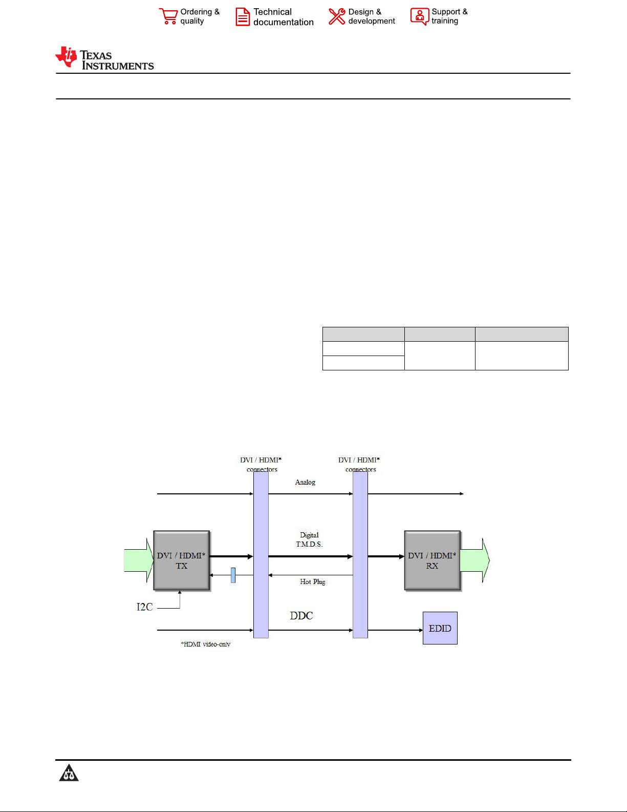
TFP401 Diagram
1
The Digital Visual Interface Specification, DVI, is an industry standard developed by the Digital Display Working Group (DDWG) for
high-speed digital connection to digital displays. The TPF401 and TFP401A are compliant with the DVI Specification Rev. 1.0.
2
The TFP401/401A has an internal voltage regulator that provides the 1.8-V core power supply from the external 3.3-V supplies.
3
The TFP401A incorporates additional circuitry to create a stable HSYNC from DVI transmitters that introduce undesirable jitter on the
transmitted HSYNC signal.
TFP401, TFP401A
SLDS120H – MARCH 2000 – REVISED MARCH 2022
An IMPORTANT NOTICE at the end of this data sheet addresses availability, warranty, changes, use in safety-critical applications,
intellectual property matters and other important disclaimers. PRODUCTION DATA.
Table of Contents
1 Features............................................................................1
2 Applications..................................................................... 1
3 Description.......................................................................1
4 Revision History.............................................................. 2
5 Description (continued).................................................. 3
6 Pin Configuration and Functions...................................3
7 Specifications.................................................................. 6
7.1 Absolute Maximum Ratings
(1)
....................................6
7.2 ESD Ratings............................................................... 6
7.3 Recommended Operating Conditions.........................6
7.4 Thermal Information....................................................6
7.5 DC Digital I/O Electrical Characteristics......................7
7.6 DC Electrical Characteristics...................................... 7
7.7 AC Electrical Characteristics.......................................7
7.8 Typical Characteristics................................................9
8 Parameter Measurement Information.......................... 10
9 Detailed Description......................................................12
9.1 Overview................................................................... 12
9.2 Functional Block Diagram......................................... 12
9.3 Feature Description...................................................12
9.4 Device Functional Modes..........................................15
10 Applications and Implementation.............................. 17
10.1 Application Information........................................... 17
10.2 Typical Application.................................................. 17
11 Power Supply Recommendations..............................20
12 Layout...........................................................................21
12.1 Layout Guidelines................................................... 21
12.2 Layout Example...................................................... 22
12.3 TI PowerPAD 100-TQFP Package..........................24
13 Device and Documentation Support..........................26
13.1 Receiving Notification of Documentation Updates..26
13.2 Support Resources................................................. 26
13.3 Trademarks.............................................................26
13.4 Electrostatic Discharge Caution..............................26
13.5 Glossary..................................................................26
14 Mechanical, Packaging, and Orderable
Information.................................................................... 26
4 Revision History
NOTE: Page numbers for previous revisions may differ from page numbers in the current version.
Changes from Revision G (May 2016) to Revision H (March 2022) Page
• Updated the numbering format for tables, figures, and cross-references throughout the document..................1
• Added row in Pin function table for thermal pad................................................................................................. 3
• Added sentence to end of first paragraph that recommends soldering package thermal pad to PCB in order to
minimize stress on peripheral pins................................................................................................................... 24
Changes from Revision F (February 2015) to Revision G (May 2016) Page
• Added t
WL(PDL_MIN)
and t
DEL
to the Section 7.7 table .........................................................................................7
Changes from Revision E (July 2013) to Revision F (February 2015) Page
• Added Pin Configuration and Functions section, ESD Ratings table, Feature Description section, Device
Functional Modes, Application and Implementation section, Power Supply Recommendations section, Layout
section, Device and Documentation Support section, and Mechanical, Packaging, and Orderable Information
section ............................................................................................................................................................... 1
TFP401, TFP401A
SLDS120H – MARCH 2000 – REVISED MARCH 2022
www.ti.com
2 Submit Document Feedback
Copyright © 2022 Texas Instruments Incorporated
Product Folder Links: TFP401 TFP401A
5 Description (continued)
PowerPAD advanced packaging technology results in best-of-class power dissipation, footprint, and ultralow
ground inductance.
The TFP401 and TFP401A combines PanelBus circuit innovation with TI's advanced 0.18-µm EPIC-5 CMOS
process technology, along with TI PowerPAD package technology to achieve a reliable, low-powered, low-noise,
high-speed digital interface solution.
6 Pin Configuration and Functions
76
77
78
79
80
81
82
83
84
85
86
87
88
89
90
91
92
93
94
95
96
97
98
99
100
51
52
53
54
55
56
57
58
59
60
61
62
63
64
65
66
67
68
69
70
71
72
73
74
75
50
49
48
47
46
45
44
43
42
41
40
39
38
37
36
35
34
33
32
31
30
29
28
27
26
25
24
23
22
21
20
19
18
17
16
15
14
13
12
11
10
9
8
7
6
5
4
3
2
1
QO1
QO0
HSYNC
DE
ODCK
OVDD
CTL3
CTL2
CTL1
GND
DVDD
QE23
QE22
QE20
QE19
QE17
QE16
OVDD
OGND
QE15
QE14
OGND
OVDD
AGND
Rx2+
Rx2−
AVDD
AGND
AVDD
Rx1−
AGND
AGND
Rx0+
Rx0−
AGND
RxC+
RxC−
AVDD
EXT_RES
PGND
RSVD
OCK_INV
QO22
QO21
QO20
QO18
QO17
QO16
GND
DVDD
QO13
QO12
Qo9
QO8
OGND
OVDD
QO7
QO6
QO5
QO4
QO3
QO2
DFO
PD
ST
PIXS
GND
DVDD
STAG
PDO
QE0
QE2
QE3
QE4
QE5
QE6
OVDD
OGND
QE9
QE11
QE12
QE13
QE7
QO23
AVDD
QO11
QO15
QO14
OGND
QE18
SCDT
QE8
QE1
QE10
QE21
VSYNC
QO10
QO19
Rx1+
PVDD
Thermal Pad
Figure 6-1. PZP Package, 100-Pin HTQFP (Top View)
Table 6-1. Pin Functions
PIN
TYPE
(1)
DESCRIPTION
NAME NO.
AGND 79, 83, 87, 89, 92 GND Analog ground – Ground reference and current return for analog circuitry
AV
DD
82, 84, 88, 95 V
DD
Analog V
DD
– Power supply for analog circuitry. Nominally 3.3 V
CTL[3:1] 42, 41, 40 DO
General-purpose control signals – Used for user-defined control. CTL1 is not powered down
via PDO.
DE 46 DO
Output data enable – Used to indicate time of active video display versus non-active display
or blank time. During blank, only HSYNC, VSYNC, and CTL[3:1] are transmitted. During
times of active display, or non-blank, only pixel data, QE[23:0], and QO[23:0] are transmitted.
High: Active display time
Low: Blank time
www.ti.com
TFP401, TFP401A
SLDS120H – MARCH 2000 – REVISED MARCH 2022
Copyright © 2022 Texas Instruments Incorporated
Submit Document Feedback
3
Product Folder Links: TFP401 TFP401A
Table 6-1. Pin Functions (continued)
PIN
TYPE
(1)
DESCRIPTION
NAME NO.
DFO 1 DI
Output clock data format – Controls the output clock (ODCK) format for either TFT or DSTN
panel support. For TFT support, the ODCK clock runs continuously. For DSTN support,
ODCK only clocks when DE is high; otherwise, ODCK is held low when DE is low.
High: DSTN support/ODCK held low when DE = low
Low: TFT support/ODCK runs continuously.
DGND 5, 39, 68 GND Digital ground – Ground reference and current return for digital core
DV
DD
6, 38, 67 V
DD
Digital V
DD
– Power supply for digital core. Nominally 3.3 V
EXT_RES 96 AI
Internal impedance matching – The TFP401/401A is internally optimized for impedance
matching at 50 Ω. An external resistor tied to this pin has no effect on device performance.
HSYNC 48 DO Horizontal sync output
RSVD 99 DI Reserved. Must be tied high for normal operation
OV
DD
18, 29, 43, 57, 78 V
DD
Output driver V
DD
– Power supply for output drivers. Nominally 3.3 V
ODCK 44 DO
Output data clock – Pixel clock. All pixel outputs QE[23:0] and QO[23:0] (if in 2-pixel/clock
mode), along with DE, HSYNC, VSYNC and CTL[3:1], are synchronized to this clock.
OGND 19, 28, 45, 58, 76 GND Output driver ground – Ground reference and current return for digital output drivers
OCK_INV 100 DI
ODCK polarity – Selects ODCK edge on which pixel data (QE[23:0] and QO[23:0]) and
control signals (HSYNC, VSYNC, DE, CTL[3:1]) are latched.
Normal mode:
High: Latches output data on rising ODCK edge
Low: Latches output data on falling ODCK edge
PD 2 DI
Power down – An active-low signal that controls the TFP401/401A power-down state. During
power down, all output buffers are switched to a high-impedance state. All analog circuits are
powered down and all inputs are disabled, except for PD.
If PD is left unconnected, an internal pullup defaults the TFP401/401A to normal operation.
High : Normal operation
Low: Power down
PDO 9 DI
Output drive power down – An active-low signal that controls the power-down state of the
output drivers. During output drive power down, the output drivers (except SCDT and CTL1)
are driven to a high-impedance state. When PDO is left unconnected, an internal pullup
defaults the TFP401/401A to normal operation.
High: Normal operation/output drivers on
Low: Output drive power down
PGND 98 GND PLL GND – Ground reference and current return for internal PLL
PIXS 4 DI
Pixel select – Selects between one- and two-pixels-per-clock output modes. During the 2-
pixel/clock mode, both even pixels, QE[23:0], and odd pixels, QO[23:0], are output in tandem
on a given clock cycle. During 1-pixel/clock, even and odd pixels are output sequentially, one
at a time, with the even pixel first, on the even pixel bus, QE[23:0]. (The first pixel per line is
pixel-0, the even pixel. The second pixel per line is pixel-1, the odd pixel).
High: 2-pixel/clock
Low: 1-pixel/clock
PV
DD
97 V
DD
PLL V
DD
– Power supply for internal PLL
QE[8:15] 20–27 DO
Even green-pixel output – Output for even and odd green pixels when in 1-pixel/clock mode.
Output for even-only green pixel when in 2-pixel/clock mode. Output data is synchronized to
the output data clock, ODCK.
LSB: QE8/pin 20
MSB: QE15/pin 27
QE[16:23] 30–37 DO
Even red-pixel output – Output for even and odd red pixels when in 1-pixel/clock mode.
Output for even-only red pixel when in 2-pixel/clock mode. Output data is synchronized to the
output data clock, ODCK.
LSB: QE16/pin 30
MSB: QE23/pin 37
QO[0:7] 49–56 DO
Odd blue-pixel output – Output for odd-only blue pixel when in 2-pixel/clock mode. Not used,
and held low, when in 1-pixel/clock mode. Output data is synchronized to the output data
clock, ODCK.
LSB: QO0/pin 49
MSB: QO7/pin 56
TFP401, TFP401A
SLDS120H – MARCH 2000 – REVISED MARCH 2022
www.ti.com
4 Submit Document Feedback
Copyright © 2022 Texas Instruments Incorporated
Product Folder Links: TFP401 TFP401A
Table 6-1. Pin Functions (continued)
PIN
TYPE
(1)
DESCRIPTION
NAME NO.
QO[8:15] 59–66 DO
Odd green-pixel output – Output for odd-only green pixel when in 2-pixel/clock mode. Not
used, and held low, when in 1-pixel/clock mode. Output data is synchronized to the output
data clock, ODCK.
LSB: QO8/pin 59
MSB: QO15/pin 66
QO[16:23] 69–75, 77 DO
Odd red-pixel output – Output for odd-only red pixel when in 2-pixel/clock mode. Not used,
and held low, when in 1-pixel/clock mode. Output data is synchronized to the output data
clock, ODCK.
LSB: QO16/pin 69
MSB: QO23/pin 77
QE[0:7] 10–17 DO
Even blue-pixel output – Output for even and odd blue pixels when in 1-pixel/clock mode.
Output for even-only blue pixel when in 2-pixel per clock mode. Output data is synchronized
to the output data clock, ODCK.
LSB: QE0/pin 10
MSB: QE7/pin 17
RxC+ 93 AI
Clock positive receiver input – Positive side of reference clock. TMDS low-voltage signal
differential input pair
RxC– 94 AI
Clock negative receiver input – Negative side of reference clock. TMDS low-voltage signal
differential input pair
Rx0+ 90 AI
Channel-0 positive receiver input – Positive side of channel-0. TMDS low-voltage signal
differential input pair.
Channel-0 receives blue pixel data in active display and HSYNC, VSYNC control signals in
blank.
Rx0– 91 AI
Channel-0 negative receiver input – Negative side of channel-0. TMDS low-voltage signal
differential input pair
Rx1+ 85 AI
Channel-1 positive receiver input – Positive side of channel-1 TMDS low-voltage signal
differential input pair
Channel-1 receives green-pixel data in active display and CTL1 control signals in blank.
Rx1– 86 AI
Channel-1 negative receiver input – Negative side of channel-1 TMDS low-voltage signal
differential input pair
Rx2+ 80 AI
Channel-2 positive receiver input – Positive side of channel-2 TMDS low-voltage signal
differential input pair
Channel-2 receives red-pixel data in active display and CTL2, CTL3 control signals in blank.
Rx2– 81 AI
Channel-2 negative receiver input – Negative side of channel-2 TMDS low-voltage signal
differential input pair
SCDT 8 DO
Sync detect - Output to signal when the link is active or inactive. The link is considered
to be active when DE is actively switching. The TFP401/401A monitors the state of DE to
determine link activity. SCDT can be tied externally to PDO to power down the output drivers
when the link is inactive.
High: Active link
Low: Inactive link
ST 3 DI
Output drive strength select – Selects output drive strength for high- or low-current drive.
(See dc specifications for I
OH
and I
OL
vs ST state).
High: High drive strength
Low: Low drive strength
STAG 7 DI
Staggered pixel select – An active-low signal used in the 2-pixel/clock pixel mode (PIXS
= high). Time-staggers the even and odd pixel outputs to reduce ground bounce. Normal
operation outputs the odd and even pixels simultaneously.
High: Normal simultaneous even/odd pixel output
Low: Time-staggered even/odd pixel output
VSYNC 47 DO Vertical sync output
Thermal Pad —
Thermal pad. Recommend soldering the package thermal pad to thermal pad on PCB.
Soldering the thermal pad will help to release stress through the solder, otherwise the stress
will be absorbed by the peripheral pins.
(1) DI = Digital Input; DO = Digital Output; AI = Analog Input; AO = Analog Output
www.ti.com
TFP401, TFP401A
SLDS120H – MARCH 2000 – REVISED MARCH 2022
Copyright © 2022 Texas Instruments Incorporated
Submit Document Feedback
5
Product Folder Links: TFP401 TFP401A
剩余32页未读,继续阅读
资源评论
Jabsun
- 粉丝: 0
- 资源: 3
上传资源 快速赚钱
- 我的内容管理 展开
- 我的资源 快来上传第一个资源
- 我的收益 登录查看自己的收益
- 我的积分 登录查看自己的积分
- 我的C币 登录后查看C币余额
- 我的收藏
- 我的下载
- 下载帮助
安全验证
文档复制为VIP权益,开通VIP直接复制
信息提交成功