没有合适的资源?快使用搜索试试~ 我知道了~
资源详情
资源评论
资源推荐
1. General description
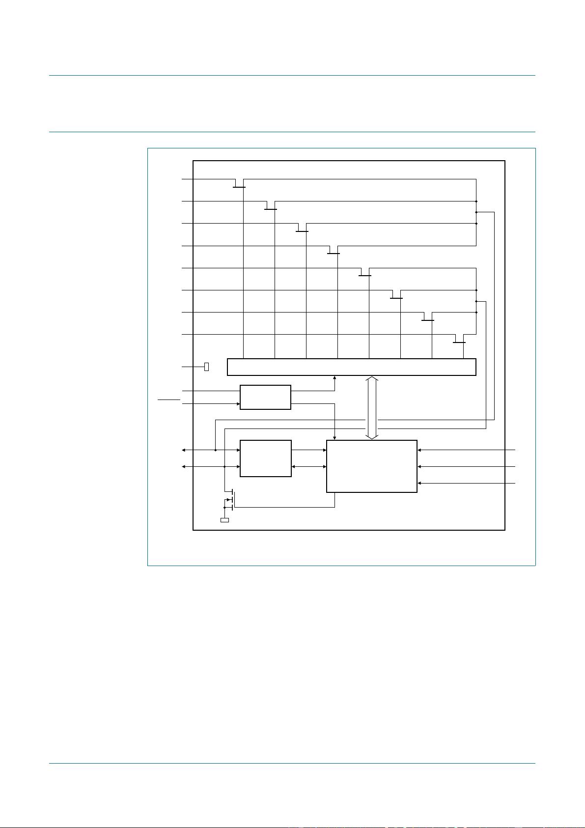
The PCA9546A is a quad bidirectional translating switch controlled via the I
2
C-bus. The
SCL/SDA upstream pair fans out to four downstream pairs, or channels. Any individual
SCx/SDx channel or combination of channels can be selected, determined by the
contents of the programmable control register.
An active LOW reset input allows the PCA9546A to recover from a situation where one of
the downstream I
2
C-buses is stuck in a LOW state. Pulling the RESET pin LOW resets
the I
2
C-bus state machine and causes all the channels to be deselected as does the
internal Power-On Reset (POR) function.
The pass gates of the switches are constructed such that the V
DD
pin can be used to limit
the maximum high voltage which is passed by the PCA9546A. This allows the use of
different bus voltages on each pair, so that 1.8 V or 2.5 V or 3.3 V parts can communicate
with 5 V parts without any additional protection. External pull-up resistors pull the bus up
to the desired voltage level for each channel. All I/O pins are 5 V tolerant.
2. Features and benefits
1-of-4 bidirectional translating switches
I
2
C-bus interface logic; compatible with SMBus standards
Active LOW reset input
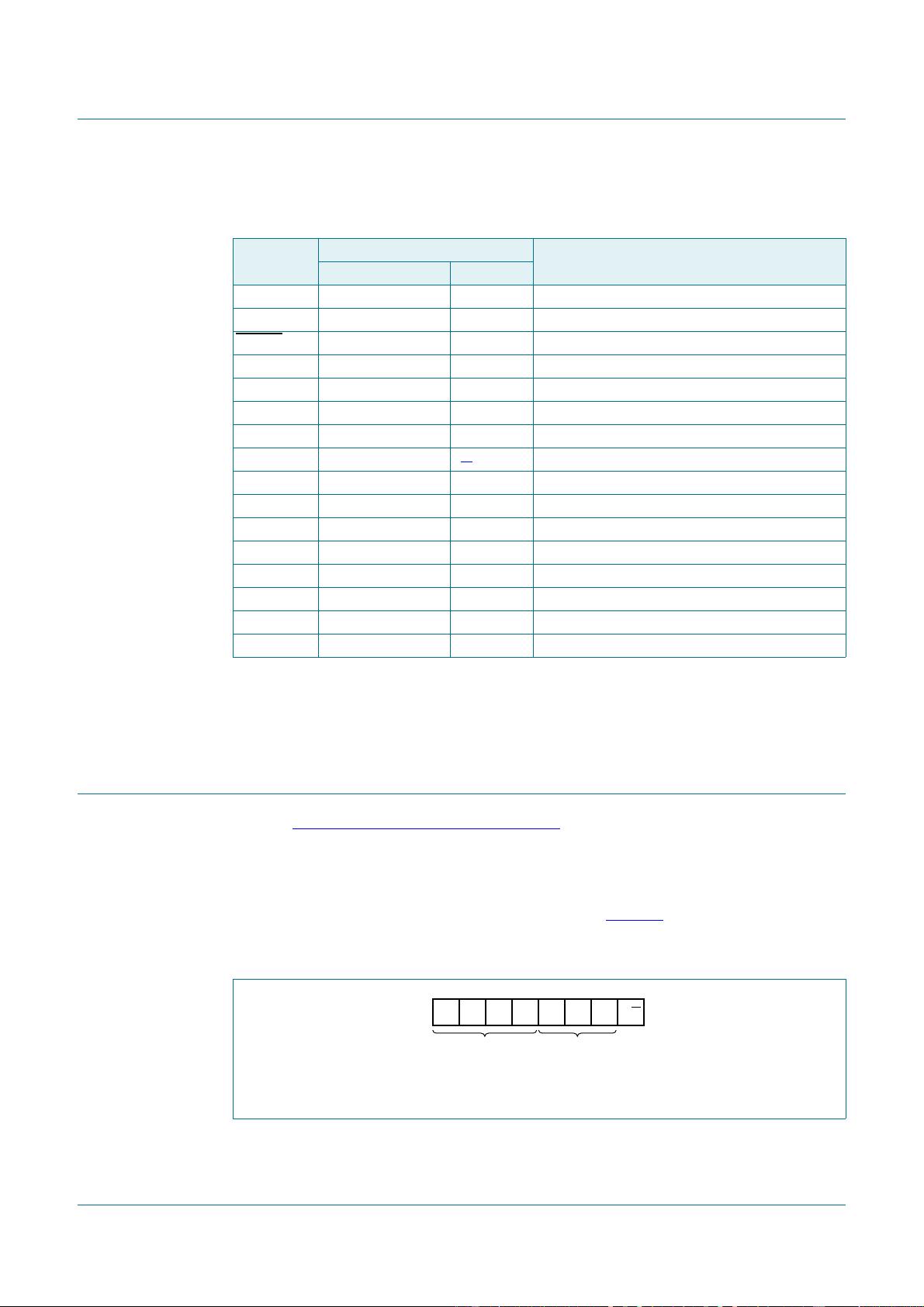
3 address pins allowing up to 8 devices on the I
2
C-bus
Channel selection via I
2
C-bus, in any combination
Power-up with all switch channels deselected
Low R
on
switches
Allows voltage level translation between 1.8 V, 2.5 V, 3.3 V and 5 V buses
No glitch on power-up
Supports hot insertion
Low standby current
Operating power supply voltage range of 2.3 V to 5.5 V
5 V tolerant Inputs
0 Hz to 400 kHz clock frequency
ESD protection exceeds 2000 V HBM per JESD22-A114 and 1000 V CDM per
JESD22-C101
Latch-up testing is done to JEDEC Standard JESD78 which exceeds 100 mA
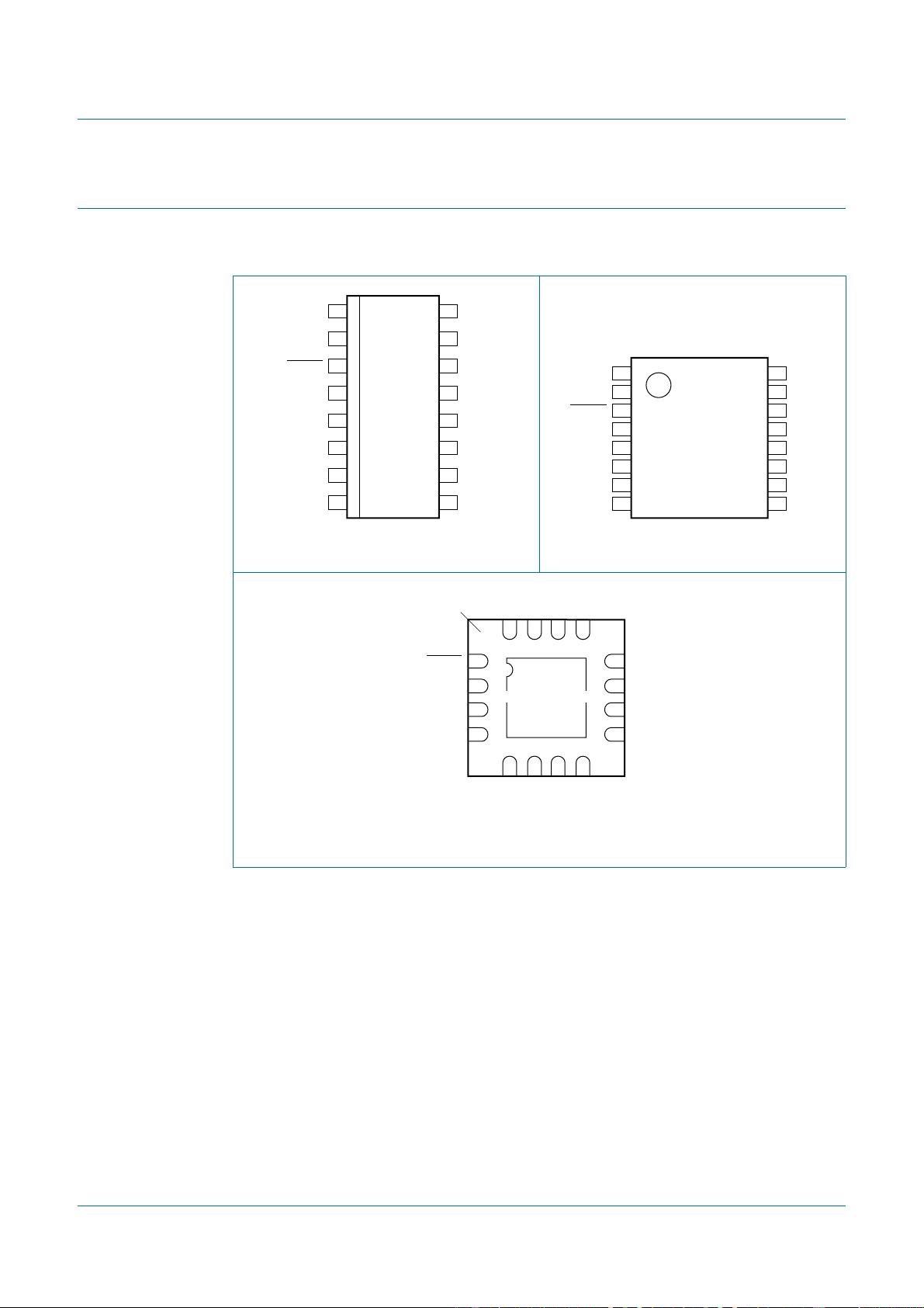
Three packages offered: SO16, TSSOP16, and HVQFN16
PCA9546A
4-channel I
2
C-bus switch with reset
Rev. 6 — 30 April 2014 Product data sheet
PCA9546A All information provided in this document is subject to legal disclaimers. © NXP Semiconductors N.V. 2014. All rights reserved.
Product data sheet Rev. 6 — 30 April 2014 2 of 30
NXP Semiconductors
PCA9546A
4-channel I
2
C-bus switch with reset
3. Ordering information
3.1 Ordering options
Table 1. Ordering information
Type number Topside
marking
Package
Name Description Version
PCA9546ABS 546A HVQFN16 plastic thermal enhanced very thin quad flat package;
no leads; 16 terminals; body 4 4 0.85 mm
SOT629-1
PCA9546AD PCA9546AD SO16 plastic small outline package; 16 leads; body width 3.9 mm SOT109-1
PCA9546APW PA9546A TSSOP16 plastic thin shrink small outline package; 16 leads;
body width 4.4 mm
SOT403-1
Table 2. Ordering options
Type number Orderable part
number
Package Packing method Minimum
order
quantity
Temperature range
PCA9546ABS PCA9546ABS,118 HVQFN16 Reel 13” Q1/T1
*Standard mark SMD
6000 T
amb
= 40 Cto+85C
PCA9546AD PCA9546AD,112 SO16 Standard marking
* IC’s tube - DSC bulk pack
1000 T
amb
= 40 Cto+85C
PCA9546AD,118 SO16 Reel 13” Q1/T1
*Standard mark SMD
2500 T
amb
= 40 Cto+85C
PCA9546APW PCA9546APW,112 TSSOP16 Standard marking
* IC’s tube - DSC bulk pack
2400 T
amb
= 40 Cto+85C
PCA9546APW,118 TSSOP16 Reel 13” Q1/T1
*Standard mark SMD
2500 T
amb
= 40 Cto+85C
PCA9546A All information provided in this document is subject to legal disclaimers. © NXP Semiconductors N.V. 2014. All rights reserved.
Product data sheet Rev. 6 — 30 April 2014 3 of 30
NXP Semiconductors
PCA9546A
4-channel I
2
C-bus switch with reset
4. Block diagram
Fig 1. Block diagram of PCA9546A
SWITCH CONTROL LOGIC
PCA9546A
POWER-ON
RESET
002aab188
SC0
SC1
SC2
SC3
SD0
SD1
SD2
SD3
V
SS
V
DD
RESET
I
2
C-BUS
CONTROL
INPUT
FILTER
SCL
SDA
A0
A1
A2
PCA9546A All information provided in this document is subject to legal disclaimers. © NXP Semiconductors N.V. 2014. All rights reserved.
Product data sheet Rev. 6 — 30 April 2014 4 of 30
NXP Semiconductors
PCA9546A
4-channel I
2
C-bus switch with reset
5. Pinning information
5.1 Pinning
Fig 2. Pin configuration for SO16 Fig 3. Pin configuration for TSSOP16
Fig 4. Pin configuration for HVQFN16 (transparent top view)
PCA9546AD
A0 V
DD
A1 SDA
RESET SCL
SD0 A2
SC0 SC3
SD1 SD3
SC1 SC2
V
SS
SD2
002aab185
1
2
3
4
5
6
7
8
10
9
12
11
14
13
16
15
PCA9546APW
A0 V
DD
A1 SDA
RESET SCL
SD0 A2
SC0 SC3
SD1 SD3
SC1 SC2
V
SS
SD2
002aab186
1
2
3
4
5
6
7
8
10
9
12
11
14
13
16
15
002aab187
Transparent top view
SD1
SD3
SC0 SC3
SD0 A2
RESET SCL
SC1
V
SS
SD2
SC2
A1
A0
V
DD
SDA
4 9
3 10
2 11
1 12
5
6
7
8
16
15
14
13
terminal 1
index area
PCA9546ABS
PCA9546A All information provided in this document is subject to legal disclaimers. © NXP Semiconductors N.V. 2014. All rights reserved.
Product data sheet Rev. 6 — 30 April 2014 5 of 30
NXP Semiconductors
PCA9546A
4-channel I
2
C-bus switch with reset
5.2 Pin description
[1] HVQFN16 package die supply ground is connected to both the V
SS
pin and the exposed center pad. The
V
SS
pin must be connected to supply ground for proper device operation. For enhanced thermal, electrical,
and board-level performance, the exposed pad must be soldered to the board using a corresponding
thermal pad on the board, and for proper heat conduction through the board thermal vias must be
incorporated in the PCB in the thermal pad region.
6. Functional description
Refer to Figure 1 “Block diagram of PCA9546A”.
6.1 Device address
Following a START condition, the bus master must output the address of the slave it is
accessing. The address of the PCA9546A is shown in Figure 5
. To conserve power, no
internal pull-up resistors are incorporated on the hardware selectable address pins and
they must be pulled HIGH or LOW.
The last bit of the slave address defines the operation to be performed. When set to
logic 1 a read is selected, while a logic 0 selects a write operation.
Table 3. Pin description
Symbol Pin Description
SO16, TSSOP16 HVQFN16
A0 1 15 address input 0
A1 2 16 address input 1
RESET
3 1 active LOW reset input
SD0 4 2 serial data 0
SC0 5 3 serial clock 0
SD1 6 4 serial data 1
SC1 7 5 serial clock 1
V
SS
86
[1]
supply ground
SD2 9 7 serial data 2
SC2 10 8 serial clock 2
SD3 11 9 serial data 3
SC3 12 10 serial clock 3
A2 13 11 address input 2
SCL 14 12 serial clock line
SDA 15 13 serial data line
V
DD
16 14 supply voltage
Fig 5. Slave address
002aab189
1 1 1 0 A2 A1 A0 R/W
fixed hardware
selectable
剩余29页未读,继续阅读
来杯清咖_
- 粉丝: 330
- 资源: 22
上传资源 快速赚钱
- 我的内容管理 展开
- 我的资源 快来上传第一个资源
- 我的收益 登录查看自己的收益
- 我的积分 登录查看自己的积分
- 我的C币 登录后查看C币余额
- 我的收藏
- 我的下载
- 下载帮助
安全验证
文档复制为VIP权益,开通VIP直接复制
信息提交成功
评论0