没有合适的资源?快使用搜索试试~ 我知道了~
FAIRCHILD-MLP14D.pdf
需积分: 5 0 下载量 152 浏览量
2023-12-12
21:18:39
上传
评论
收藏 1.03MB PDF 举报
温馨提示
试读
16页
FAIRCHILD-MLP14D
资源推荐
资源详情
资源评论
© 2005 Fairchild Semiconductor Corporation www.fairchildsemi.com
USBIT1103 Universal Serial Bus Peripheral Transceiver with Voltage Regulator
October 2007
USB1T1103 Rev. 1.0.3
USB1T1103
Universal Serial Bus Peripheral Transceiver
with Voltage Regulator
Features
■ Complies with Universal Serial Bus Specification 2.0
■ Integrated 5V to 3.3V voltage regulator for powering
VBus
■ Utilizes digital inputs and outputs to transmit and
receive USB cable data
■ Supports full speed (12Mbits/s) data rates
■ Ideal for portable electronic devices
■ MLP technology package (16 terminal) with HBCC
footprint
■ 15kV contact HBM ESD protection on bus terminals
■ Supports disable mode and is functionally equivalent
to Philips ISP1102
Applications
■ PDA
■ PC Peripherals
■ Cellular Phones
■ MP3 Players
■ Digital Still Camera
■ Information Appliance
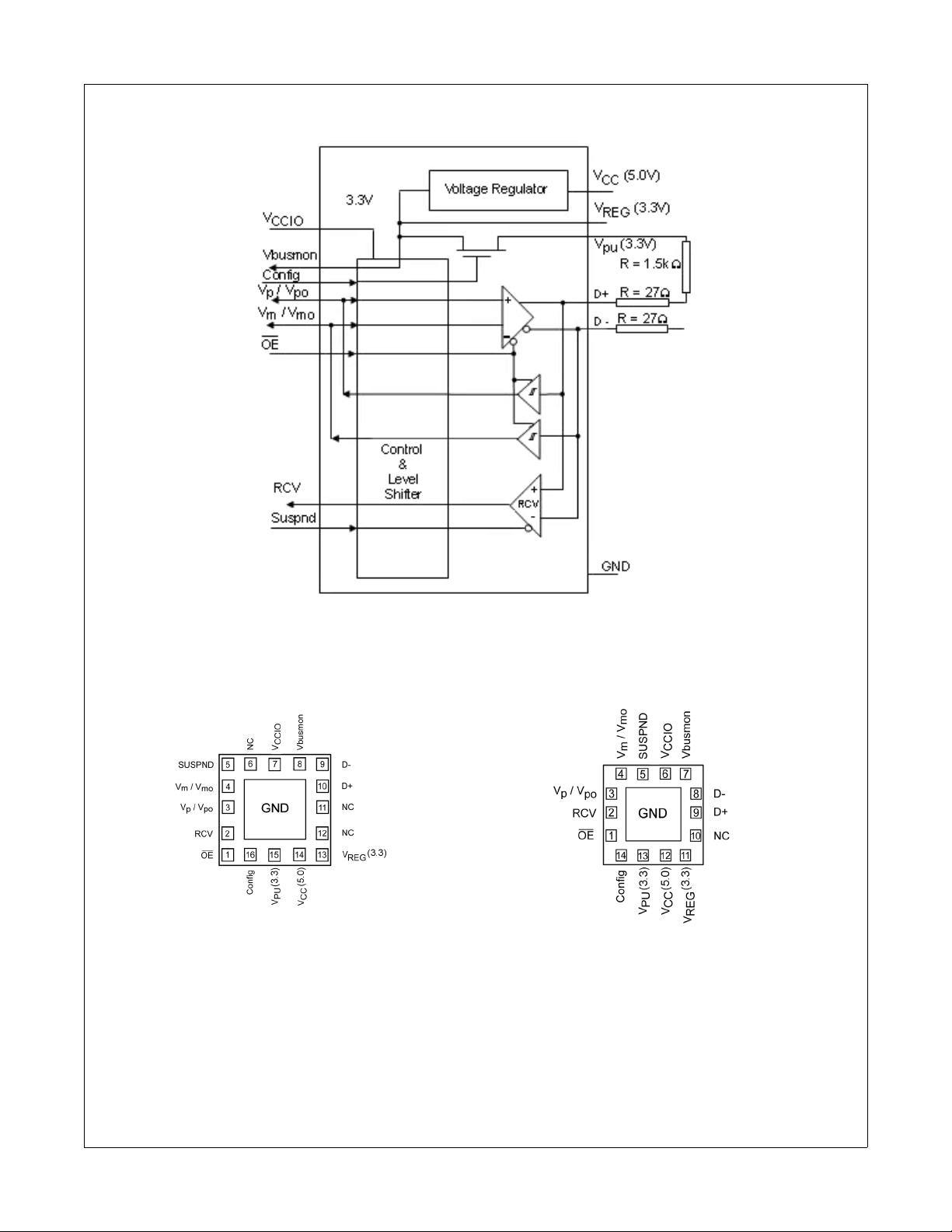
Description
This chip provides a USB Transceiver functionality with a
voltage regulator that is compliant to USB Specification
Rev 2.0. this integrated 5V to 3.3V regulator allows inter-
facing of USB Application specific devices with supply
voltages ranging from 1.65V to 3.6V with the physical
layer of Universal Serial Bus. It is capable of operating at
12Mbits/s (full speed) data rates and hence is fully com-
pliant to USB Specification Rev 2.0. The Vbusmon termi-
nal allows for monitoring the Vbus line.
The USB1T1103 also provides exceptional ESD protec-
tion with 15kV contact HBM on D+,D- terminals
Ordering Information
Pb-Free package per JEDEC J-STD-020B.
Part Number Package
Number
Product code
Top Mark
Pb-Free Package Description Packing
Method
USB1T1103MPX
MLP14D $Y&Z&2&T
USB1103
Yes 14-Terminal Molded Leadless Package
(MLP), 2.5mm Square
3K Units
on Tape
and Reel
USB1T1103MHX
MLP16HB $Y&Z&2&T
USB1103
Yes 16-Terminal Molded Leadless Package
(MHBCC), JEDEC MO-217,3mm
Square
3K Units
on Tape
and Reel
USB1T1103 Universal Serial Bus Peripheral Transceiver with Voltage Regulator
© 2005 Fairchild Semiconductor Corporation www.fairchildsemi.com
USB1T1103 Rev. 1.0.3 2
Typical Application
Figure 1. Logic Diagram
Connection Diagrams
Figure 2. MLP16 GND Exposed Diepad
(Bottom View)
Figure 3. MLP14 GND Exposed Diepad
(Bottom View)
USB1T1103 Universal Serial Bus Peripheral Transceiver with Voltage Regulator
© 2005 Fairchild Semiconductor Corporation www.fairchildsemi.com
USB1T1103 Rev. 1.0.3 3
Terminal Descriptions
Terminal
Number
Terminal
Name
I/O Terminal Description
MLP14 MLP16
1 1 OE I Output Enable:
Active LOW enables the transceiver to transmit data on the bus. When not active the transceiver is in
the receive mode (CMOS level is relative to V
CCIO
)
2 2 RCV O Receive Data Output:
Non-inverted CMOS level output for USB differential Input (CMOS output level is relative to V
CCIO
).
Driven LOW when SUSPN is HIGH; RCV output is stable and preserved during SE0 condition.
33V
p
/V
po
I/O Single-ended D+ receiver output V
P
(CMOS level relative to V
CCIO
):
Used for external detection of SE0, error conditions, speed of connected device; Terminal also acts
as drive data input V
po
(see Table 1 and Table 2).
Output drive is 4 mA buffer.
44V
m
/V
mo
I/O Single-ended D- receiver output V
m
(CMOS level relative to V
CCIO
):
Used for external detection of SE0, error conditions, speed of connected device; Terminal also acts
as drive data input V
mo
(see Table 1 and Table 2).
Output drive is 4 mA buffer.
5 5 SUSPND I Suspend:
Enables a low power state (CMOS level is relative to V
CCIO
). While the
SUSPND terminal is active (HIGH) it will drive the RCV terminal to logic “0” state.
— 6 NC No Connect
67V
CCIO
Supply Voltage for digital I/O terminals (1.65V to 3.6V):
When not connected the D+ and D- terminals are in 3-STATE. This supply bus is totally independent
of V
CC
(5V) and V
REG
(3.3V), and must never exceed the V
REG
(3.3) voltage. For V
CCIO
discon-
nected the O+/O- terminals are HIGH Impedance and the V
PU
(3.3V) is turned off.
7 8 Vbusmon O Vbus monitor output (CMOS level relative to V
CCIO
):
When Vbus > 4.1V then Vbusmon = HIGH and when Vbus < 3.6V then
Vbusmon = LOW. If SUSPND = HIGH then Vbusmon is pulled HIGH.
9, 8 10, 9 D+, D- AI/O Data +, Data -:
Differential data bus conforming to the USB standard. Terminals are HIGH Impedance for bus pow-
ered mode when Vbus < 3.6V. For ByPass Mode then HIGH Impedance when V
REG
/ Vbus < V
REG
minimum.
10 11 NC No Connect
— 12 NC No Connect
11 13 V
REG
(3.3V) Internal Regulator Option:
Regulated supply output voltage (3.0V to 3.6V) during 5V operation;
decoupling capacitor of at least 0.1 µF is required.
Regulator ByPass Option:
Used as supply voltage input for 3.3V operation.
12 14 V
CC
(5.0V) Internal Regulator Option:
Used as supply voltage input (4.0V to 5.5V); can be connected directly to USB line Vbus.
Regulator ByPass Option:
Connected to V
REG
(3.3V)
13 15 V
PU
(3.3V) Pull-up Supply Voltage (3.3V ± 10%):
Connect an external 1.5kΩ resistor on D+ (FS data rate);
Terminal function is controlled by Config input terminal:
Config = LOW - V
PU
(3.3V) is floating (HIGH Impedance) for zero pull-up current.
Config = HIGH - V
PU
(3.3V) = 3.3V; internally connected to V
REG
(3.3V).
V
PU
is OFF in disable mode.
14 16 Config I USB connect or disconnect software control input.
Configures 3.3V to external 1.5kΩ resistor on D+ when HIGH.
Exposed
Diepad
Exposed
Diepad
GND GND GND supply down bonded to exposed diepad to be connected to the PCB GND.
USB1T1103 Universal Serial Bus Peripheral Transceiver with Voltage Regulator
© 2005 Fairchild Semiconductor Corporation www.fairchildsemi.com
USB1T1103 Rev. 1.0.3 4
Functional Description
The USB1T1103 transceiver is designed to convert
CMOS data into USB differential bus signal levels and to
convert USB differential bus signal to CMOS data.
To minimize EMI and noise the outputs are edge rate
controlled with the rise and fall times controlled and
defined for full speed data rates only (12Mbits/s). The
rise, fall times are balanced between the differential ter-
minals to minimize skew.
The USB1T1103 differs from earlier USB Transceiver in
that the V
p
/V
m
and V
po
/V
mo
terminals are now I/O termi-
nals rather than discrete input and output terminals.
Table 1 describes the specific terminal functionality
selection. Table 2 and Table 3 describe the specific Truth
Tables for Driver and Receiver operating functions.
The USB1T1103 also has the capability of various power
supply configurations, including a disable mode for
V
CCIO
disconnected, to support mixed voltage supply
applications (see Table 4) and Section 2.1 for detailed
descriptions.
Functional Tables
Table 1. Function Select
Notes:
1. Signal levels is function of connection and/or pull-up/pull-down resistors.
2. For SUSPND = HIGH mode the differential receiver is inactive and the output RCV is forced LOW. The out-of-suspend signaling
(K) is detected via the single-ended receivers of the V
p
/V
po
and V
m
/V
mo
terminals.
Table 2. Driver Function (OE = L) using Differential Input Interface
Notes:
3. SE0 = Single Ended Zero
Table 3. Receiver Function (OE = H)
Notes:
4. X = Don't Care
5. RCV(0) denotes the signal level on output RCV just prior to the SE0 or SE1 event. This level is stable during the SE0 or SE1
event period.
SUSPND OE D+, D- RCV
V
p
/V
po
V
m
/V
mo
Function
L L Driving &
Receiving
Active V
po
Input V
mo
Input Normal Driving
(Differential Receiver Active)
L H Receiving
(1)
Active V
p
Output V
m
Output Receiving
H L Driving Inactive
(2)
V
po
Input V
mo
Input Driving during Suspend
(Differential Receiver Inactive)
HH3 STATE
(1)
Inactive
(2)
V
p
Output V
m
Output Low Power State
V
m
/V
mo
V
p
/V
po
Data (D+ / D-)
L L SE0
(3)
L H Differential Logic 1
H L Differential Logic 0
H H Illegal State
D+, D- RCV
V
p
/V
po
V
m
/V
mo
Differential Logic 1 H H L
Differential Logic 0 L L H
SE0 X L L
剩余15页未读,继续阅读
资源评论
硬件小白成长中
- 粉丝: 516
- 资源: 22
上传资源 快速赚钱
- 我的内容管理 展开
- 我的资源 快来上传第一个资源
- 我的收益 登录查看自己的收益
- 我的积分 登录查看自己的积分
- 我的C币 登录后查看C币余额
- 我的收藏
- 我的下载
- 下载帮助
安全验证
文档复制为VIP权益,开通VIP直接复制
信息提交成功