504
• 2023 IEEE International Solid-State Circuits Conference
ISSCC 2023 / SESSION 34 / CRYO-CMOS FOR QUANTUM COMPUTING / 34.1
34.1 THz Cryo-CMOS Backscatter Transceiver: A Contactless
4 Kelvin-300 Kelvin Data Interface
Jinchen Wang, Mohamed I. Ibrahim, Isaac B. Harris, Nathan M. Monroe,
Muhammad Ibrahim Wasiq Khan, Xiang Yi, Dirk R. Englund, Ruonan Han
Massachusetts Institute of Technology, Cambridge, MA
Modern low-temperature large-scale systems, such as high-sensitivity IR/THz imaging
arrays and quantum computers, require massive signal connections between the cooled
system core and external room-temperature (RT) components. An error-protected
quantum computer needs thousands or even millions of qubits operating at cryogenic
temperature. Albeit the rapid development of highly-integrated quantum processors [1],
future scalability may still be largely limited by the cables connecting the processors and
peripheral control/processing units [2]; because even using low-thermal-conductivity
metal materials, those cables still transport non-negligible amount of heat due to the
large temperature gradient. In a dilution refrigerator, a stainless-steel UT-085-SS-SS
cable could pose close to one mW of heat load to the 4K stage, and tens of mW to the
50K stage [2]. To drive such a non-copper cable in the cryogenic-to-RT (i.e. uplink) data
path, standard I/O circuits in cooled sensors/processors typically consume pJ/b-level
energy, further raising the overall heat load. Recently, optical fibers along with cryogenic
InGaAs photodiode [3] and VCSEL lasers [4] are used for <20mK coherent qubit
control/readout mode and 4K-to-300K uplink data mode, respectively. The energy
consumption in [4] reduces to 406.2fJ/b at 10Gbps and <10
-12
bit-error-rate (BER). In
this paper, a terahertz (THz) transceiver chip operating at 4K is presented as a CMOS-
based, fully-integrable alternative to the interconnect solutions above. The carrier
frequency of 260GHz, which is determined based on the trade-off between the antenna
dimension and the efficiency of the transistors, is sufficiently high to minimize the link
footprint and to avoid potential disturbance of qubits, such as the superconducting or
nitrogen-vacancy ones, that typically operate at gigahertz; on the other hand, it also leads
to much lower quantum noise (~ħω ) compared to that in photonic links. The transceiver
avoids the power-hungry terahertz (THz) generation by adopting a passive backscatter
communication scheme (Fig. 34.1.1), and a 4Gbps uplink is demonstrated with only
176fJ/b added heat load. In the downlink, the heat load is further reduced to 34fJ/b at
4.4Gbps. This fully contactless 4K-RT interface can be used to deliver digitized
control/readout data, and even some analog/RF signals such as low phase noise clocks.
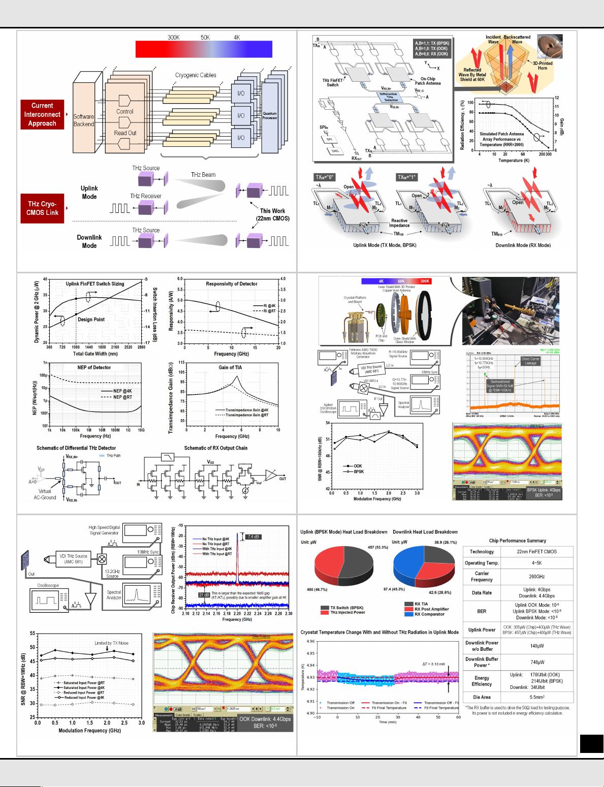
The architecture of the chip is shown in Fig. 34.1.2, which is based on a 2×2 quad-feed
patch antenna array. Each patch has a square shape, leading to an identical resonance
frequency of 260GHz for waves polarized in either X- or Y- directions. Three orthogonal
edges of the patch are connected through a pair of FinFET switches M
1
, M
2
and
wavelength (λ)-long transmission lines TL
1
, TL
2
. The fourth edge of the patch is
connected to a THz detector. In the uplink mode, the detector is deactivated and presents
a reactive impedance that reflects any antenna-received wave back. The uplink mode is
enabled when the digital control A,B=1,1. Shown in Fig. 34.1.2, in this mode, the THz
switches are toggled by the uplink input data TX
IN
, and the incident wave polarized in the
Y-direction excites the antenna TM
010
mode. When TX
IN
=0, the wave is routed via TL
1
and M
1
to the left edge of the patch and then re-radiated through the antenna TM
100
mode
with polarization in the X-direction. In this state, the disconnected M
2
and the λ-long TL
2
present open to the top edge of the patch, hence avoiding disturbance to the backscatter
process. Similarly, when TX
IN
=1, the wave is routed to the right edge of the patch, but
now the re-radiated wave possesses the opposite phase. The compact antenna structure
therefore realizes binary phase-shift keying (BPSK) modulation and cross polarization
in the backscatter communication; the latter reduces direct leakage from the THz source
to the THz receiver located at 300K (Fig. 34.1.1).
Note that the power consumption of the uplink is dominated by the CV
2
f dynamic power
of the THz switches. Narrower switch reduces such power, but increases the THz power
dissipation inside the switch, which also adds heat load. Based on the simulated data in
Fig. 34.1.3, the switch width is set to 1.08µm. In Fig. 34.1.2, with A,B=1,0, M
1
is always
OFF, and the chip can operate in on/off keying (OOK) uplink mode, which leads to higher
BER but lower dynamic switching power. Lastly, we note that the link budget of
backscatter communication is proportional to the square of antenna radiation efficiency
η, which is only 38% at 300K. Fortunately, with the large electrical conductivity increase
of copper at 4K, the simulated η improves to 97% (Fig. 34.1.2). To achieve a larger
radiation aperture and to avoid out-of-aperture THz power injection into the cryostat, a
custom-designed horn antenna with a large flange shield is implemented using 3D metal
printing. It is placed at the 60K stage in front of the chip without physical contact.
In the downlink mode, the digital control A,B=0,0 turns off both M
1
and M
2
(Fig. 34.1.2),
which then leads to open termination at three edges of the patch. Meanwhile, A=0
activates the THz square-law detector pair shown in Fig. 34.1.3 by applying a gate bias
V
GS
through an inverter. Exciting the TM
010
mode of the antennas, the incident wave is
injected differentially into the THz detector. Based on a cold-FET detector topology, the
detector at 4K achieves ~4.5A/W current responsivity and ~0.13pW/Hz
1/2
noise equivalent
power (NEP) in the simulation while consuming zero power. The faster device response,
lower thermal noise and higher antenna efficiency lead to a ~500x sensitivity increase
compared to that operating at 300K. In Fig. 34.1.3, the detector bias node is a virtual
ground created by the differential THz input signal, which prevents the impact of
parasitics at that node on the THz detector. The 260GHz downlink carrier is OOK
modulated. After the demodulation, the baseband signals from the detector pair become
in-phase and are then injected into a chain of 80dBΩ transimpedance (TIA) amplifier,
limit amplifier and a comparator. For testing purpose, a buffer stage is added for 50Ω
matching to the external instruments; it is not required in a future fully integrated
cryogenic chip system.
The chip is fabricated using the Intel 22nm FinFET process and is designed with device
models at 4K. The die size is 5.5mm
2
. The chip is attached to a round PCB with a diameter
of 28mm, which is then mounted to the 4K cold-finger of a cryostat (Fig. 34.1.4). The
THz radiation is coupled into and out of the chip through a horn antenna and the glass
window of the cryostat. The setup of the uplink measurement (Fig. 34.1.4) utilizes a VDI
amplifier-multiplier chain (AMC-681) to generate the 260GHz carrier, and a VDI sub-
harmonic mixer to demodulate the backscattered wave. Their horn antennas are placed
with orthogonal E-planes. Single-tone signal and pseudo-random binary sequence
(PRBS) data are fed into the chip from an arbitrary waveform generator. Figure 34.1.4
shows the down-converted BPSK backscatter spectrum, which gives a single-sideband
SNR of 52.5dB at 100kHz resolution bandwidth (RBW) and indicates sufficient link
budget for multi-Gbps transmission. Figure 34.1.4 also shows the SNR over various
switching frequencies, as well as an eye diagram of demodulated BPSK data when a
4Gbps PRBS is fed to the chip. At 4Gbps, the OOK and BPSK modes provide <10
-6
and
<10
-8
BER while consuming 305µW and 457µW of power, respectively. By monitoring
the temperature rise of the cryostat with and without the external THz source (Fig.
34.1.6), we determine that the THz power injected into the cryostat is ~400µW (with
~50µW uncertainty), resulting in an overall heat load of 176fJ/b (OOK) and 214fJ/b
(BPSK).
In the downlink measurement (Fig. 34.1.5), reduced THz power injection (<10µW) is
performed to avoid chip receiver saturation, and the ~11GHz input of the VDI-AMC is
OOK modulated. First, with the VDI-AMC turned off, we see that the measured noise floor
of the chip receiver output is reduced by 21dB from RT to 4K (Fig. 34.1.5). Then, with
the VDI-AMC turned on, the chip receiver output power increases by 7.4dB from RT to
4K. These two values verify our previous prediction of 500x sensitivity improvement at
4K. With THz input, the noise floor at both temperatures is however all elevated, indicating
that the SNR of the downlink (i.e. 49dB maximum at RBW=1MHz) is already limited by
the noise of the VDI-AMC radiation, not the chip itself. Figure 34.1.5 shows an eye
diagram of the chip output when the AMC is driven by a 4.4Gbps PRBS, and corresponds
to a BER below 10
-8
. The downlink chip power is 149W and the injected THz power is
negligible, which leads to a heat load of 34fJ/bit. The heat load introduced by the horn
antenna or the glass window is too small to be measured accurately. The performance
of the work is summarized in Fig. 34.1.6. In light of the rapid advances of on-chip THz
sources and receivers at room temperature [5], an all-silicon THz cryogenic link interface
should be feasible in the future. The extensibility towards larger system sizes may also
benefit by replacing free space coupling with thermal insulating THz dielectric-waveguide
link [6].
Acknowledgement:
The chip is fabricated through Intel University Shuttle Program. The authors also thank
Prof. Jelena Notaros and Daniel DeSantis of MIT for the support of test instruments.
References:
[1] E. Charbon et al., “Cryo-CMOS Circuits and Systems for Scalable Quantum
Computing,” ISSCC, pp. 264-265, Feb. 2017.
[2] S. Krinner et al., “Engineering Cryogenic Setups for 100-Qubit Scale Superconducting
Circuit Systems,” EPJ Quantum Technology, vol. 6, no. 2, 2019.
[3] W. Fu et al., “Superconducting Processor Modulated VCSELs for 4K High-Speed
Optical Data Link,” IEEE J. Quantum Electronics, vol. 58, no. 2, Apr. 2022.
[4] F. Lecocq et al., “Control and Readout of a Superconducting Qubit Using a Photonic
Link,” Nature, vol. 591, pp. 575-579, Mar. 2021.
[5] K. Sengupta et al., “Terahertz Integrated Electronics and Hybrid Electronic-Photonic
Systems,”Nature Electronics1, pp. 622-635, 2018.
[6] J. W. Holloway et al., “Cryo-CMOS Circuits and Systems for Scalable Quantum
Computing,” ISSCC, pp. 196-197, Feb. 2021.
978-1-6654-9016-0/23/$31.00 ©2023 IEEE