
ADS1210
ADS1211
24-Bit ANALOG-TO-DIGITAL CONVERTER
FEATURES
● DELTA-SIGMA A/D CONVERTER
● 23 BITS EFFECTIVE RESOLUTION AT 10Hz
AND 20 BITS AT 1000Hz
● DIFFERENTIAL INPUTS
● PROGRAMMABLE GAIN AMPLIFIER
● FLEXIBLE SPI
™
-COMPATIBLE SSI
INTERFACE WITH 2-WIRE MODE
● PROGRAMMABLE CUT-OFF FREQUENCY
UP TO 15.6kHz
● INTERNAL/EXTERNAL REFERENCE
● ON-CHIP SELF-CALIBRATION
● ADS1211 INCLUDES 4-CHANNEL MUX
DESCRIPTION
The ADS1210 and ADS1211 are precision, wide dynamic
range, delta-sigma Analog-to-Digital (A/D) converters with
24-bit resolution operating from a single +5V supply. The
differential inputs are ideal for direct connection to transduc-
ers or low-level voltage signals. The delta-sigma architec-
ture is used for wide dynamic range and to ensure 22 bits
of no-missing-code performance. An effective resolution of
23 bits is achieved through the use of a very low-noise input
amplifier at conversion rates up to 10Hz. Effective resolu-
tions of 20 bits can be maintained up to a sample rate of
1kHz through the use of the unique Turbo modulator mode
of operation. The dynamic range of the converters is further
increased by providing a low-noise programmable gain
amplifier with a gain range of 1 to 16 in binary steps.
The ADS1210 and ADS1211 are designed for high resolution
measurement applications in smart transmitters, industrial
process control, weigh scales, chromatography, and portable
instrumentation. Both converters include a flexible synchro-
nous serial interface that is SPI-compatible and also offers a
two-wire control mode for low cost isolation.
The ADS1210 is a single-channel converter and is offered in
both 18-pin DIP and 18-lead SOIC packages. The ADS1211
includes a 4-channel input multiplexer and is available in 24-
pin DIP, 24-lead SOIC, and 28-lead SSOP packages.
APPLICATIONS
● INDUSTRIAL PROCESS CONTROL
● INSTRUMENTATION
● BLOOD ANALYSIS
● SMART TRANSMITTERS
● PORTABLE INSTRUMENTS
● WEIGH SCALES
● PRESSURE TRANSDUCERS
A
D
S
1
2
1
0
A
D
S
1
2
1
1
A
D
S
1
2
1
0
ADS1211
A
D
S
1
2
1
1
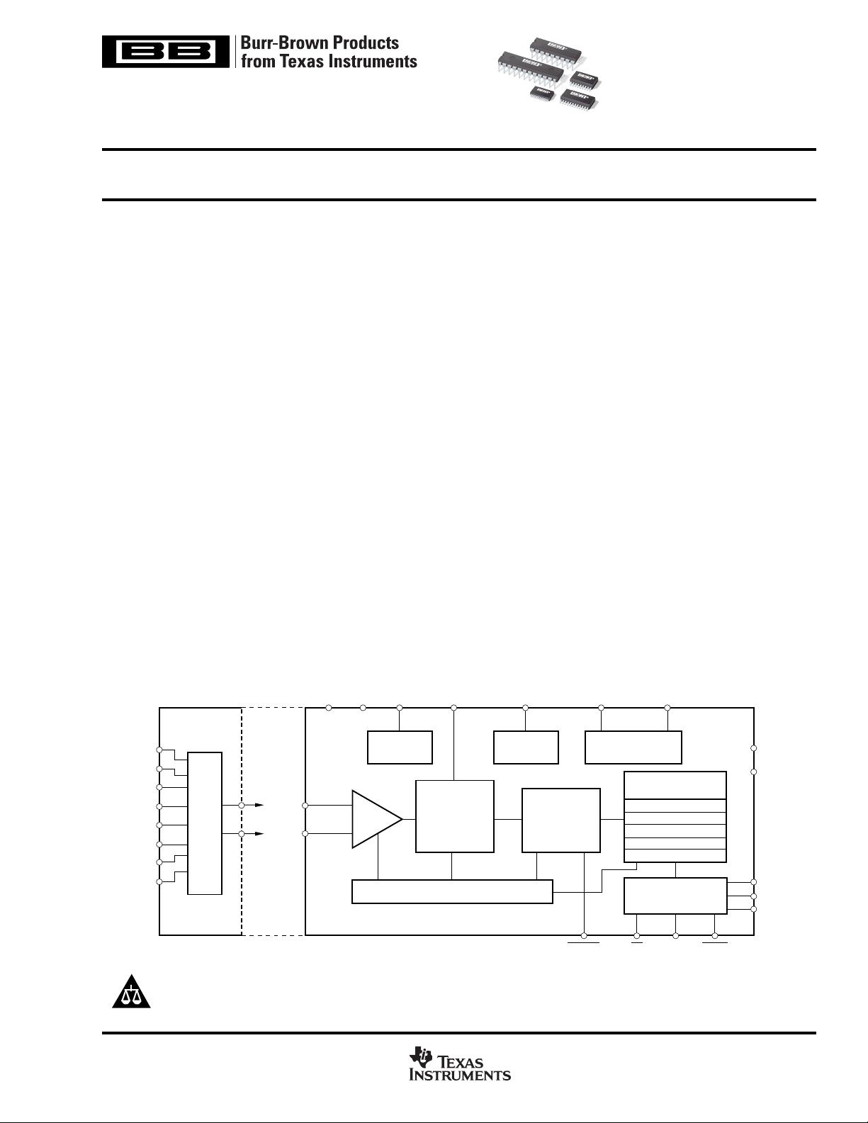
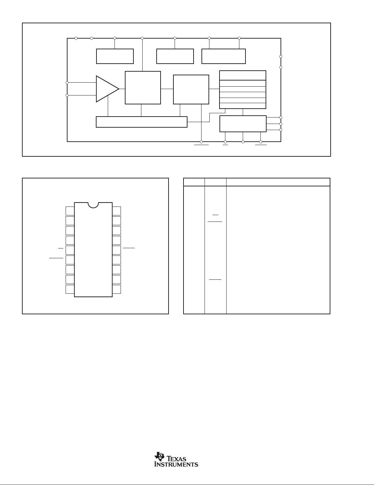
PGA
+2.5V
Reference
+3.3V Bias
Generator
Clock Generator
Serial Interface
Second-Order
∆∑
Modulator
Instruction Register
Command Register
Data Output Register
Offset Register
Full-Scale Register
Third-Order
Digital Filter
Micro Controller
Modulator Control
AGND AV
DD
REF
OUT
REF
IN
V
BIAS
X
IN
X
OUT
MODE
DSYNCADS1211 Only ADS1210/11 CS DRDY
A
IN
P
A
IN
N
SCLK
DGND
DV
DD
SDIO
SDOUT
MUX
A
IN
1P
A
IN
1N
A
IN
2P
A
IN
2N
A
IN
3P
A
IN
3N
A
IN
4P
A
IN
4N
SBAS034B – JANUARY 1996 – REVISED SEPTEMBER 2005
www.ti.com
PRODUCTION DATA information is current as of publication date.
Products conform to specifications per the terms of Texas Instruments
standard warranty. Production processing does not necessarily include
testing of all parameters.
Copyright © 1996-2005, Texas Instruments Incorporated
Please be aware that an important notice concerning availability, standard warranty, and use in critical applications of
Texas Instruments semiconductor products and disclaimers thereto appears at the end of this data sheet.
All trademarks are the property of their respective owners.

剩余48页未读,继续阅读
资源评论


weixin_44191002
- 粉丝: 1
- 资源: 1


最新资源
- 21考试真题最近的t387.txt
- 21考试真题最近的t386.txt
- 21考试真题最近的t385.txt
- 21考试真题最近的t384.txt
- 21考试真题最近的t383.txt
- 21考试真题最近的t382.txt
- 21考试真题最近的t381.txt
- 21考试真题最近的t380.txt
- 21考试真题最近的t379.txt
- 21考试真题最近的t378.txt
- 21考试真题最近的t377.txt
- 22考试真题最近的t1.txt
- python158基于旅游网站的数据分析及可视化系统(flask)wlw 该这个了.zip
- python154基于opencv的疲劳检测系统(django).zip
- 22考试真题最近的t2.txt
- 22考试真题最近的t3.txt
资源上传下载、课程学习等过程中有任何疑问或建议,欢迎提出宝贵意见哦~我们会及时处理!
点击此处反馈


