具有看门狗功能的TPL5010芯片资料

需积分: 0 99 浏览量
更新于2024-01-13
收藏 903KB PDF 举报
TPL5010 芯片资料知识点总结
TPL5010 芯片是一款超低功耗计时器,具有看门狗功能,广泛应用于单片机、嵌入式系统、STM32 等领域。下面是 TPL5010 芯片的详细知识点总结:
一、电源电压范围和电流消耗
TPL5010 芯片的电源电压范围为 1.8V 至 5.5V,典型电流消耗为 35nA,该芯片拥有超低功耗特性,非常适合电池供电系统和物联网 (IoT) 等应用场景。
二、计时器精度和时间间隔
TPL5010 芯片的计时器精度为 1%(典型值),可选计时间隔为 100ms 至 7200s,用户可以通过电阻选择时间间隔,满足不同应用场景的需求。
三、看门狗功能
TPL5010 芯片具有看门狗功能,可以监控系统的运行状态,当系统出现故障或超时时,TPL5010 芯片可以发出警报或重启系统,该功能广泛应用于安全、监控、自动化等领域。
四、应用场景
TPL5010 芯片的应用场景非常广泛,包括电池供电系统、物联网 (IoT)、出入探测、篡改检测、家庭自动化传感器、温度调节装置、消费类电子产品、远程传感器等领域。
五、封装和尺寸
TPL5010 芯片采用 6 引脚小外形尺寸晶体管 (SOT23) 封装,尺寸为 3.00mm × 3.00mm,非常适合小型化和轻量化的设计。
六、器件信息
TPL5010 芯片的器件信息包括器件编号、封装尺寸、引脚数量、工作温度范围等信息,用户可以根据实际需求选择合适的器件。
七、Pin 配置和功能
TPL5010 芯片的 Pin 配置和功能包括电源引脚、时钟引脚、数据引脚、复位引脚等,用户可以根据需要配置 Pin,以满足不同的应用场景。
八、技术规格
TPL5010 芯片的技术规格包括绝对最大 ratings、ESD 等级、Recommended Operating Ratings 等信息,用户可以根据实际需求选择合适的技术规格。
TPL5010 芯片是一款功能强大、体积小巧、功耗超低的计时器芯片,广泛应用于单片机、嵌入式系统、STM32 等领域,用户可以根据实际需求选择合适的器件和技术规格。
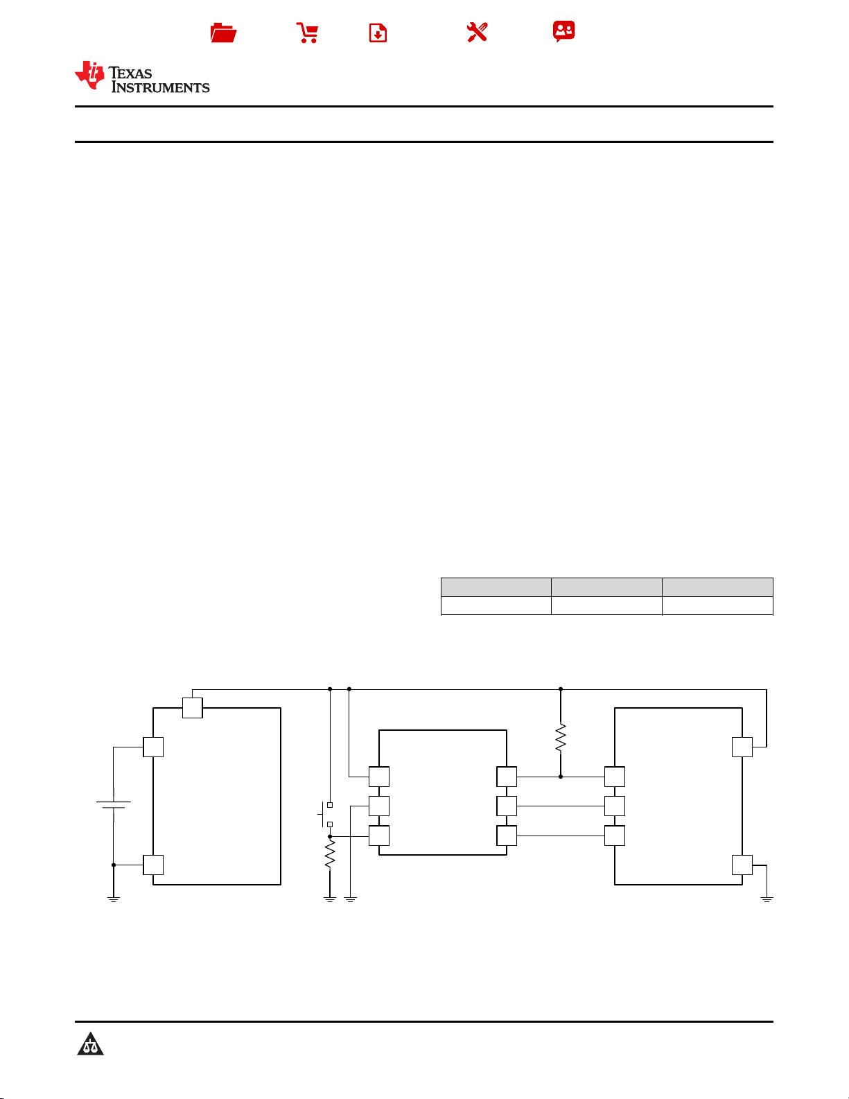
VIN
POWER MANAGEMENT
VOUT
GND
µC
GPIO
VDD
GND
Rp
GPIO
RSTn
TPL5010
VDD
GND
RSTn
WAKE
DELAY/
M_RST
DONE
R
EXT
Battery
-+
Product
Folder
Order
Now
Technical
Documents
Tools &
Software
Support &
Community
本文档旨在为方便起见,提供有关 TI 产品中文版本的信息,以确认产品的概要。 有关适用的官方英文版本的最新信息,请访问 www.ti.com,其内容始终优先。 TI 不保证翻译的准确
性和有效性。 在实际设计之前,请务必参考最新版本的英文版本。
English Data Sheet: SNAS651
TPL5010
ZHCSEK6A –JANUARY 2015–REVISED SEPTEMBER 2018
具具有有看看门门狗狗功功能能的的 TPL5010 纳纳瓦瓦级级功功耗耗系系统统计计时时器器
1
1 特特性性
1
• 电源电压范围为 1.8V 至 5.5V
• 电压为 2.5V 时,电流消耗为 35nA(典型值)
• 可选计时间隔:100ms 至 7200s
• 计时器精度:1%(典型值)
• 可通过电阻选择时间间隔
• 看门狗功能
• 手动复位
2 应应用用
• 电池供电系统
• 物联网 (IoT)
• 出入探测
• 篡改检测
• 家庭自动化传感器
• 温度调节装置
• 消费类电子产品
• 远程传感器
• 白色家电
3 说说明明
TPL5010 纳瓦级计时器是一款超低功耗计时器,其看
门狗功能专为占空比、电池供电型 应用 (比如物联网
中的应用)中的系统唤醒功能而设计。其中许多 应用
需要使用 μC,因此,通常希望将 μC 维持在低功耗模
式以更大限度节省电流,而仅在某些时间间隔内唤醒以
收集数据或为中断提供服务。虽然 μC 的内部计时器可
用于系统唤醒,但它可能单独消耗数微安的总系统电
流。
TPL5010 仅消耗 35nA,可替代集成式 μC 计时器的功
能。这样就可将 μC 置于低得多的功耗模式,将内部计
时器关闭,并在被 TPL5010 中断时仅返回到激活模
式。TPL5010 通过提供近两个数量级的功率节省,可
以大幅减小能量采集或无线传感器 应用中所使用的电
池尺寸。TPL5010 提供 100ms 至 7200s 的可选时间
间隔,适用于中断驱动型 应用。出于安全考虑,某些
标准(如 EN50271)要求实现看门狗功能。TPL5010
不仅实现了看门狗功能,而且几乎没有增加功耗。
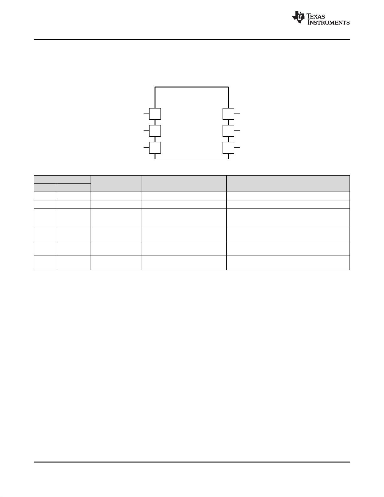
TPL5010 采用 6 引脚小外形尺寸晶体管 (SOT23) 封
装。
器器件件信信息息
(1)
器器件件编编号号 封封装装 封封装装尺尺寸寸((标标称称值值))
TPL5010 SOT23 (6) 3.00mm × 3.00mm
(1) 如需了解所有可用封装,请参阅产品说明书末尾的可订购产品
附录。
简简化化应应用用电电路路原原理理图图


剩余26页未读,继续阅读
2020-10-22 上传
2021-01-19 上传
2013-03-12 上传
2017-12-23 上传
2010-09-11 上传
2022-11-30 上传
185 浏览量
2020-08-28 上传
115 浏览量
2010-11-09 上传
109 浏览量
107 浏览量
2021-01-13 上传
118 浏览量
169 浏览量
2013-08-30 上传
146 浏览量
2021-01-12 上传
2019-08-28 上传
2021-04-19 上传
资源评论


操控者
- 粉丝: 49
- 资源: 3


最新资源
- 猪行为自动化视频分析技术在群体水平高度关联于人工观测的行为活动-畜牧业动物福利监测新方法
- JAVA求链表长度的递归方法,这个想法是通过维护一个函数来使用递归
- 生成二维码.html
- comsol裂隙注浆模拟,案例 考虑三层顶板包含随机裂隙的浆液扩散模型,考虑浆液重力的影响,建立随机裂隙,采用达西定律模块,分析不同注浆压力条件下的浆液扩散规律,建立瞬态模型 可以明显看到随着时间变
- JAVA源码+SpringBoot+vue+mysql 大学城水电管理系统 +数据库+文档
- 、comsol中相场方法模拟多孔介质中驱替的计算案例 提供采用相场方法模拟多孔介质中驱替的算例,可在此基础上学会多孔介质中的驱替模拟,得到水驱油(或其他两相)后多孔介质中的残余油分布,计算采出程度随时
- 基于椭圆拟合的粘连仔猪灰度图像自动分割算法及应用(用于仔猪体重监测系统)
- EV录屏是一款集视频录制与直播功能于一身的桌面录屏软件,支持多种录制模式
- Java install
- JAVA源码+SpringBoot+vue+mysql 体育馆管理系统 +数据库+文档
- 多孔介质多相流,水驱油模型,达西两相流模型comsol
- 新能源汽车 电力系统 优化 基于粒子群算法的电动汽车群有序充电优化 设计简介:解决与电动汽车充电站的电力分配相关的问题 通过使用粒子群优化(PSO)算法,为电动汽车充电站找到最优的充电策略,以最小化
- 小零件打包机捆包机sw18可编辑全套技术资料100%好用.zip
- JAVA源码+SpringBoot+vue+mysql 健身房管理系统 +数据库+文档
- C# 自定义控件 opencvsharp 卡尺测距
- 电驱动(电机+电控)开发验证方法与技巧讲授 精讲 细讲 教程,高清视频课程
