没有合适的资源?快使用搜索试试~ 我知道了~
ISL83490IBZ-T
0 下载量 17 浏览量
2024-03-12
14:53:16
上传
评论
收藏 1.02MB PDF 举报
温馨提示
试读
19页
ISL83490IBZ-T数据手册
资源推荐
资源详情
资源评论
FN6052 Rev.5.00 Page 1 of 19
Nov 21, 2018
FN6052
Rev.5.00
Nov 21, 2018
ISL83483, ISL83485, ISL83488, ISL83490, ISL83491
3.3V, Low Power, High Speed or Slew Rate Limited, RS-485/RS-422 Transceivers
DATASHEET
These Renesas RS-485/RS-422 devices are BiCMOS 3.3V
powered, single transceivers that meet both the RS-485 and
RS-422 standards for balanced communication. Unlike
competitive devices, this Renesas family is specified for 10%
tolerance supplies (3V to 3.6V).
The ISL83483
and ISL83488 use slew rate limited drivers
which reduce EMI, and minimize reflections from improperly
terminated transmission lines, or unterminated stubs in
multidrop and multipoint applications.
Data rates up to 10Mbps are achievable by using the
ISL83485
, ISL83490, or ISL83491, which feature higher
slew rates.
Logic inputs (for example, DI and DE) accept signals in
excess of 5.5V, making them compatible with 5V logic
families.
Receiver (Rx) inputs feature a “fail-safe if open” design,
which ensures a logic high output if Rx inputs are floating. All
devices present a “single unit load” to the RS-485 bus, which
allows up to 32 transceivers on the network.
Driver (Tx) outputs are short-circuit protected, even for
voltages exceeding the power supply voltage. Additionally,
on-chip thermal shutdown circuitry disables the Tx outputs to
prevent damage if power dissipation becomes excessive.
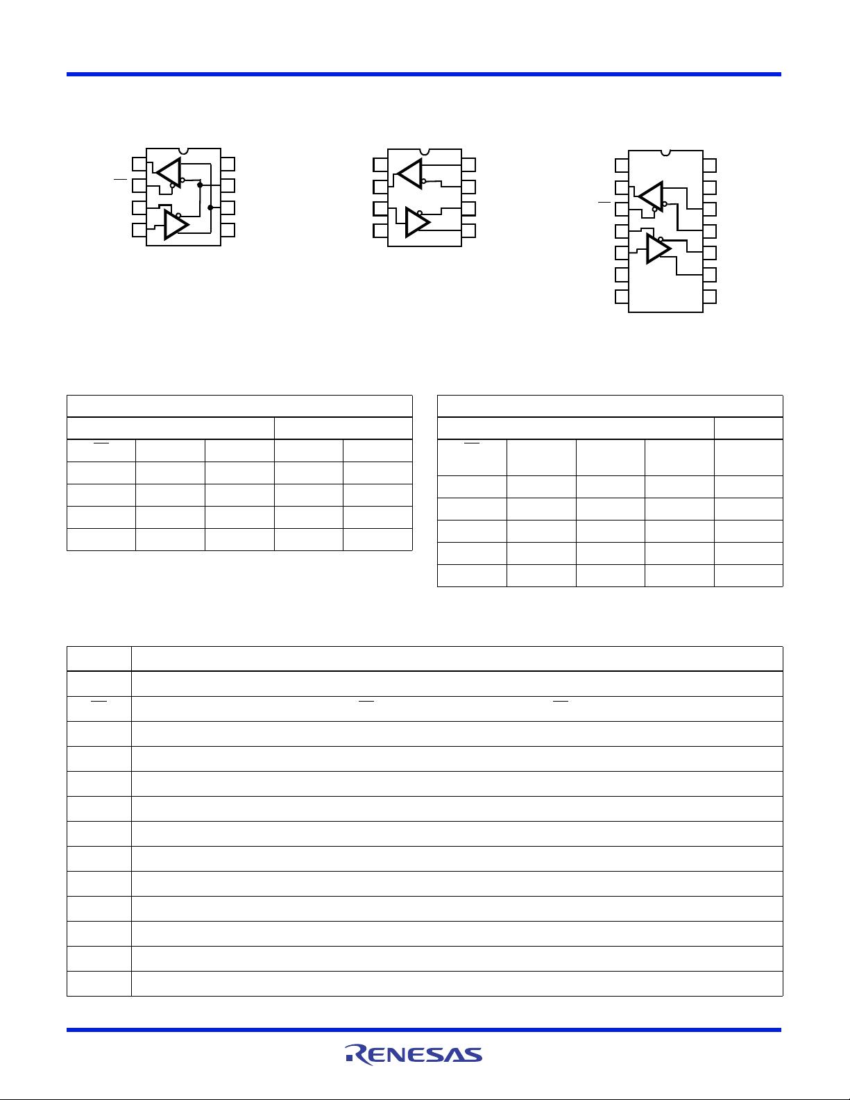
The ISL83488, ISL83490, and ISL83491 are configured for
full duplex (separate Rx input and Tx output pins)
applications. The ISL83488 and ISL83490 are offered in
space saving 8 Ld packages for applications not requiring Rx
and Tx output disable functions (for example, point-to-point
and RS-422). Half duplex configurations (ISL83483,
ISL83485) multiplex the Rx inputs and Tx outputs to provide
transceivers with Rx and Tx disable functions in 8 Ld
packages.
Features
• Operate from a single +3.3V supply (10% tolerance)
• Interoperable with 5V logic
• High data rates. . . . . . . . . . . . . . . . . . . . . . up to 10Mbps
• Single unit load allows up to 32 devices on the bus
• Slew rate limited versions for error free data transmission
(ISL83483, ISL83488) . . . . . . . . . . . . . . . . .up to 250kbps
• Low current Shutdown mode (ISL83483, ISL83485,
ISL83491). . . . . . . . . . . . . . . . . . . . . . . . . . . . . . . . . .15nA
• -7V to +12V common-mode input voltage range
• Three-state Rx and Tx outputs (except ISL83488,
ISL83490)
• 10ns propagation delay, 1ns skew (ISL83485, ISL83490,
ISL83491)
• Full duplex and half duplex pinouts
• Current limiting and thermal shutdown for driver overload
protection
• Pb-free (RoHS compliant)
Applications
• Factory automation
• Security networks
• Building environmental control systems
• Industrial/process control networks
• Level translators (for example, RS-232 to RS-422)
• RS-232 “Extension Cords”
Related Literature
For a full list of related documents, visit our website:
• ISL83483, ISL83485, ISL83488, ISL83490, ISL83491
device pages
TABLE 1. SUMMARY OF FEATURES
PART
NUMBER
HALF/FULL
DUPLEX
DATA RATE
(Mbps)
SLEW-RATE
LIMITED?
RECEIVER/DRIVER
ENABLE?
QUIESCENT I
CC
(mA)
LOW POWER
SHUTDOWN? PIN COUNT
ISL83483 Half 0.25 Yes Yes 0.65 Yes 8
ISL83485 Half 10 No Yes 0.65 Yes 8
ISL83488 Full 0.25 Yes No 0.65 No 8
ISL83490 Full 10 No No 0.65 No 8
ISL83491 Full 10 No Yes 0.65 Yes 14
ISL83483, ISL83485, ISL83488, ISL83490, ISL83491
FN6052 Rev.5.00 Page 2 of 19
Nov 21, 2018
Ordering Information
PART NUMBER
(Notes 2
, 3)
PART
MARKING TEMP. RANGE (°C)
TAPE AND REEL
(UNITS) (Note 1) PACKAGE
PKG.
DWG. #
ISL83483IBZ 83483 IBZ -40 to +85 - 8 Ld SOIC (RoHS compliant) M8.15
ISL83483IBZ-T 83483 IBZ -40 to +85 2.5k 8 Ld SOIC (RoHS compliant) M8.15
ISL83483IBZ-T7A 83483 IBZ -40 to +85 250 8 Ld SOIC (RoHS compliant) M8.15
ISL83483IP (No longer available or supported) ISL 83483IP -40 to +85 - 8 Ld PDIP E8.3
ISL83485IBZ 83485 IBZ -40 to +85 - 8 Ld SOIC (RoHS compliant) M8.15
ISL83485IBZ-T 83485 IBZ -40 to +85 2.5k 8 Ld SOIC (RoHS compliant) M8.15
ISL83485IBZ-T7A 83485 IBZ -40 to +85 250 8 Ld SOIC (RoHS compliant) M8.15
ISL83488IBZ 83488 IBZ -40 to +85 - 8 Ld SOIC (RoHS compliant) M8.15
ISL83488IBZ-T 83488 IBZ -40 to +85 2.5k 8 Ld SOIC (RoHS compliant) M8.15
ISL83490IBZ 83490 IBZ -40 to +85 - 8 Ld SOIC (RoHS compliant) M8.15
ISL83490IBZ-T 83490 IBZ -40 to +85 2.5k 8 Ld SOIC (RoHS compliant) M8.15
ISL83491IBZ 83491IBZ -40 to +85 - 14 Ld SOIC (RoHS compliant) M14.15
ISL83491IBZ-T 83491IBZ -40 to +85 2.5k 14 Ld SOIC (RoHS compliant) M14.15
ISL83491IBZ-T7A 83491IBZ -40 to +85 250 14 Ld SOIC (RoHS compliant) M14.15
ISL83491IP (No longer available, recommended
replacement: ISL83491IBZ)
ISL83491IP -40 to +85 - 14 Ld PDIP E14.3
NOTES:
1. Refer to TB347
for details about reel specifications.
2. These Pb-free plastic packaged products employ special Pb-free material sets, molding compounds/die attach materials, and 100% matte tin
plate plus anneal (e3 termination finish, which is RoHS compliant and compatible with both SnPb and Pb-free soldering operations). Pb-free
products are MSL classified at Pb-free peak reflow temperatures that meet or exceed the Pb-free requirements of IPC/JEDEC J STD-020.
3. For Moisture Sensitivity Level (MSL), refer to the ISL83483
, ISL83485, ISL83488, ISL83490, and ISL83491 device pages. For more information
about MSL, refer to TB363
.
ISL83483, ISL83485, ISL83488, ISL83490, ISL83491
FN6052 Rev.5.00 Page 3 of 19
Nov 21, 2018
Pinouts
ISL83483, ISL83485 (PDIP, SOIC)
TOP VIEW
ISL83488, ISL83490 (SOIC)
TOP VIEW
ISL83491 (PDIP, SOIC)
TOP VIEW
NOTE: PDIP packages are no longer supported
RO
RE
DE
DI
1
2
3
4
8
7
6
5
V
CC
B/Z
A/Y
GND
D
R
V
CC
RO
DI
GND
1
2
3
4
8
7
6
5
A
B
Z
Y
D
R
NC
RO
RE
DE
DI
GND
GND
V
CC
V
CC
A
B
Z
Y
NC
1
2
3
4
5
6
7
14
13
12
11
10
9
8
D
R
Truth Tables
TRANSMITTING
INPUTS OUTPUTS
RE
DE DI Z Y
X1101
X1010
0 0 X High-Z High-Z
1 0 X High-Z * High-Z *
NOTE: *Shutdown Mode for ISL83483, ISL83485, ISL83491
RECEIVING
INPUTS OUTPUT
RE
DE
Half Duplex
DE
Full Duplex
A-B RO
0 0 X ≥ +0.2V 1
0 0 X ≤ -0.2V 0
0 0 X Inputs Open 1
100XHigh-Z *
1 1 1 X High-Z
NOTE: *Shutdown Mode for ISL83483, ISL83485, ISL83491
Pin Descriptions
PIN FUNCTION
RO Receiver output: If A > B by at least 0.2V, RO is high; If A < B by 0.2V or more, RO is low; RO = High if A and B are unconnected (floating).
RE
Receiver output enable. RO is enabled when RE is low; RO is high impedance when RE is high.
DE Driver output enable. The driver outputs, Y and Z, are enabled by bringing DE high. They are high impedance when DE is low.
DI Driver input. A low on DI forces output Y low and output Z high. Similarly, a high on DI forces output Y high and output Z low.
GND Ground connection.
A/Y Noninverting receiver input and noninverting driver output. Pin is an input if DE = 0; pin is an output if DE = 1.
B/Z Inverting receiver input and inverting driver output. Pin is an input if DE = 0; pin is an output if DE = 1.
A Noninverting receiver input.
B Inverting receiver input.
Y Noninverting driver output.
Z Inverting driver output.
V
CC
System power supply input (3V to 3.6V).
NC No Connection.
ISL83483, ISL83485, ISL83488, ISL83490, ISL83491
FN6052 Rev.5.00 Page 4 of 19
Nov 21, 2018
Typical Operating Circuits
For calculating the resistor values refer to TB509, “Detecting Bus Signals Correctly with Failsafe Biased RS-485 Receivers”
FIGURE 1. ISL83483, ISL83485
FIGURE 2. ISL83488, ISL83490
FIGURE 3. ISL83491
3.3V
R
B
R
T2
R
B
V
FS
RO
RE
DE
DI
A/Y
B/Z
1
2
3
4
5
GND
V
CC
7
6
8
100nF
R
PU
3.3V
R
T1
RO
RE
DE
DI
A/Y
B/Z
1
2
3
4
5
GND
V
CC
7
6
8
100nF
R
PU
3.3V
R
T
RO
DI
A
B
2
3
GND
V
CC
7
8
1
100nF
R
T
4
Z
Y5
6
3.3V
RO
DI
A
B
2
3
GND
V
CC
7
8
1
100nF
4
Z
Y5
6
3.3V
RO
DI
A
B
2
5
GND
V
CC
11
12
13, 14
100nF
6, 7
Z
Y9
10
3.3V
100nF
RE
DE
3
4
RO
DI
A
B
2
5
GND
V
CC
11
10
13,14
6, 7
Z
Y9
12
RE
DE
3
4
R
PU
R
PU
R
B
R
T
R
B
R
B
R
T
R
B
剩余18页未读,继续阅读
资源评论
recoverlittlebylittle
- 粉丝: 1
- 资源: 20
上传资源 快速赚钱
- 我的内容管理 展开
- 我的资源 快来上传第一个资源
- 我的收益 登录查看自己的收益
- 我的积分 登录查看自己的积分
- 我的C币 登录后查看C币余额
- 我的收藏
- 我的下载
- 下载帮助
安全验证
文档复制为VIP权益,开通VIP直接复制
信息提交成功