


DACx050 1 +
±
R
G1
VREFIO
Bipolar
Output
+
±
R
G3
R
2
Signal
Input
Signal
Output
Serial
Interface
OPAMP
OPAMP
VOUT
DAC
Register
DAC
Buffer
BUF
Power Down Logic
Resistive Network
Interface Logi c
Power On Reset
VREFIO
SCLK or SCL
SDIN or SDA
SYNC
AGND
VDD
DAC
Internal
Reference
SPI2C
or A0
Product
Folder
Order
Now
Technical
Documents
Tools &
Software
Support &
Community
An IMPORTANT NOTICE at the end of this data sheet addresses availability, warranty, changes, use in safety-critical applications,
intellectual property matters and other important disclaimers. PRODUCTION DATA.
DAC80501
,
DAC70501
,
DAC60501
SBAS794D –NOVEMBER 2018–REVISED FEBRUARY 2020
DACx0501 16-Bit, 14-Bit, and 12-Bit, 1-LSB INL, Voltage-Output DACs
With Precision Internal Reference
1
1 Features
1
• 16-bit performance: 1-LSB INL and DNL (max)
• Low glitch energy: 4 nV–s
• Wide power supply: 2.7 V to 5.5 V
• Buffered output range: 5 V, 2.5 V, or 1.25 V
• Very-low power: 1 mA at 5.5 V
• Integrated 5-ppm/˚C (max), 2.5-V precision
reference
• Pin-selectable serial interface:
– 3-wire, SPI compatible up to 50-MHz
– 2-wire, I
2
C compatible
• Power-on-reset: Zero scale or midscale
• 1.62-V VIH with VDD = 5.5 V
• Temperature range: –40˚C to +125˚C
• Packages: Small 8-Pin WSON and 10-Pin VSSOP
2 Applications
• Oscilloscope (DSO)
• Semiconductor test
• Data acquisition (DAQ)
• LCD test
• Small cell base station
• Analog output module
• Process analytics (pH, gas, concentration, force
and humidity)
• DC power supply, ac source, electronic load
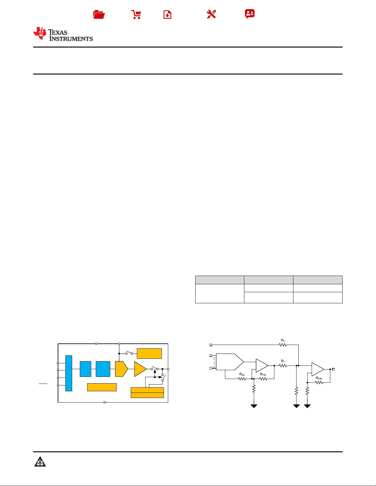
3 Description
The 16-bit DAC80501, 14-bit DAC70501, and 12-bit
DAC60501 (DACx0501) digital-to-analog converters
(DACs) are highly accurate, low-power devices with
voltage-output. The DACx0501 are specified
monotonic by design, and offer linearity of < 1 LSB.
These devices include a 2.5-V, 5-ppm/˚C internal
reference, giving full-scale output voltage ranges of
1.25 V, 2.5 V, or 5 V. The DACx0501 incorporate a
power-on-reset circuit that makes sure the DAC
output powers up at zero scale or midscale, and
remains at that scale until a valid code is written to
the device. These devices consume a low current of
1 mA, and include a power-down feature that reduces
current consumption to typically 15 µA at 5 V.
The digital interface of the DACx0501 can be
configured to SPI or I
2
C mode using the SPI2C pin.
In SPI mode, the DACx0501 use a versatile 3-wire
serial interface that operates at clock rates of up to
50 MHz. In I
2
C mode, the DACx0501 operate in
standard (100 kbps), fast (400 kbps), and fast+
(1.0 Mbps) modes.
The DACx0501 are available in easy-to-assemble
10-pin VSSOP and small 2-mm × 2-mm, 8-pin WSON
packages. The devices are fully specified over the
industrial temperature range of –40°C to +125°C.
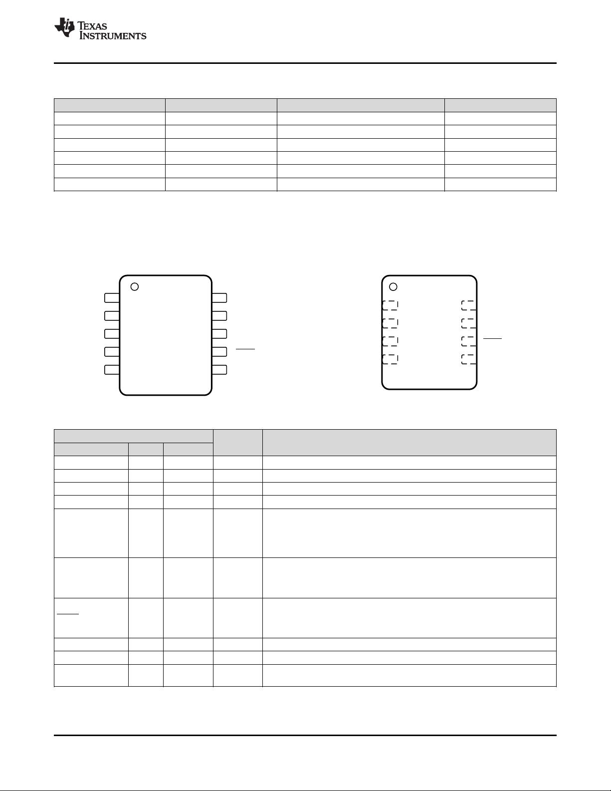
Device Information
(1)
PART NUMBER PACKAGE BODY SIZE (NOM)
DAC80501
DAC70501
DAC60501
WSON (8) 2.00 mm × 2.00 mm
VSSOP (10) 3.00 mm × 3.00 mm
(1) For all available packages, see the package option addendum
at the end of the data sheet.
Functional Block Diagram Offset Trimming With the DACx0501


- 1
- 2
- 3
前往页