Asynchronous FIFO V4.0Asynchronous FIFO V4.0
2 October 4, 2001
the read or the write clock domain, or two independent
counts can be enabled, one for each clock domain.
Synchronization and Timing Issues
As previously stated, the read and write ports can be oper-
ated on independent asynchronous clock domains. How-
ever, the user interface logic still must address
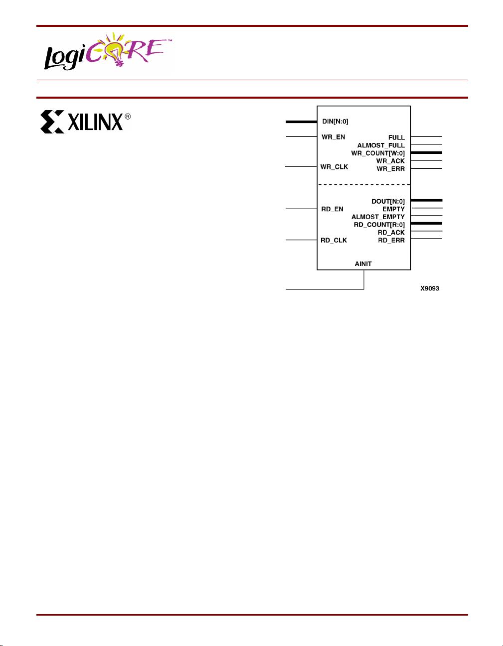
synchronization issues. The core schematic symbol,
shown in Figure 1, divides the signals according to their
appropriate clock domains—write on the top half, read on
the bottom. All signals, either input or output, are synchro-
nous to one of the two clocks, with the exception of AINIT,
which performs an asynchronous reset of the entire FIFO.
On the write side, the control (WR_EN) and data input
(DIN) are sampled by the rising edge of WR_CLK and
should be synchronous to the WR_CLK. For the read side
the read control (RD_EN) should be synchronous to the
RD_CLK and the output data (DOUT) is valid after the sub-
sequent rising edge of RD_CLK. All status outputs are syn-
chronous to their respective clock domains and should be
sampled only by logic operating on a synchronous clock.
FIFO performance can be effectively constrained and ana-
lyzed by placing the desired clock PERIOD constraints on
both the WR_CLK and RD_CLK source signals.
WR_CLK and RD_CLK are always rising edge active for
the FIFO core. They can be made falling edge active (rela-
tive to the clock source) by inserting an inverter between
the clock source and the FIFO’s clock inputs.
Behavior of Status Signals
The activation of the AINIT, asynchronous initialization
(reset), will force all four FIFO flags to the active (high)
state. On the first WR_CLK after the release of AINIT the
FULL and ALMOST_FULL flags will become inactive, indi-
cating that the FIFO is now ready to accept write opera-
tions. EMPTY and ALMOST_EMPTY are deactivated on a
rising edge of the RD_CLK following the first and second
writes respectively. The ALMOST_EMPTY flag is active
whentheFIFOhasonedatawordorisEMPTY.The
ALMOST_FULLflagisactivewhentheFIFOhasonlyone
available memory location or is FULL.
Optional handshake signals are provided to simplify user
control logic interacting with the FIFO. The WR_ACK and
WR_ERR signals indicate acknowledgment or rejection of
requested write operations. Similarly, RD_ACK and
RD_ERR signals indicate the acknowledgment or rejection
of read operations. Each of these control signals can be
made active high or low from the GUI. Note that all of these
handshake signals are synchronous to their respective
clock domains and indicate the acknowledgment or rejec-
tion of requests during the prior rising clock edge. Because
an acknowledgment or error response depends on an
active request (WR_EN or RD_EN), the ACK and ERR sig-
nals are not always the inverse of each other. If no opera-
tion is requested, both the acknowledgment and the error
signal will be inactive during the subsequent clock period.
For an example of expected signal sequencing, refer to the
timing diagram shown in Figure 2.
The optional data count outputs (WR_COUNT and
RD_COUNT) support the generation of user programma-
ble flags. In the simplest case, selecting a width of one for a
data count produces a half-full flag. Like all other FIFO out-
puts, the counts are synchronized to their respective clock
domains and should be sampled only by logic operating on
the same (or a synchronous) clock. The data count vectors
have clock latency and should not be used as substitutes
for the FULL, ALMOST_FULL, EMPTY, or ALMOST
_EMPTY flags. The clock latency of the counts in their
respective clock domains is one cycle. For example, the
WR_COUNT does not reflect the impact of a write opera-
tion performed as a result of a request (WR_EN active) dur-
ing the prior clock cycle. The latency for operations in the
opposing clock domain can be up to three clock cycles. For
example, in the case of the WR_COUNT, read operations
that may have been performed during the immediate three
prior RD_CLK periods will not be reflected in the data count
vector. This latency results from a design trade-off between
clock frequency and count accuracy and is not as limiting
as it may at first appear.
Consider the following scenario of a FIFO configured depth
of 63 and a write count of two bits (WR_COUNT[1:0]).
Note that for this example:
Write_COUNT[1:0]=00: Indicates that the FIFO is less than
1/4 full and corresponds to the occupancy range of (0:16).
The upper bound is 16 and not 15 due to the write latency
of 1 clock cycle.
Write_COUNT[1:0]=01: Indicates that the FIFO is between
1/4 full and 1/2 full and corresponds to the occupancy
range of (13:32). The lower bound is 13 and not 16 due to
the read latency of 3 clock cycles.
Write_COUNT[1:0]=10: Indicates that the FIFO is between
1/2 full and 3/4 full and corresponds to the occupancy
range of (29-48).
Write_COUNT[1:0]=11: Indicates that the FIFO is between
3/4 full and full and corresponds to the occupancy range of
(45-63).
If the control logic needs to throttle back write operations
based on the FIFO occupancy, it can use the write count
vector in the following way. As shown above,
WR_COUNT[1:0] equal to 11 corresponds to an occupancy
greater than 45. As long as the user’s WR_COUNT is not
11, no more than 48 data words (47 plus one for the write
operation clock latency) are present in the FIFO. The user’s
control logic is assured that at least 15 (63-48) additional
memory locations are available in the queue. There could
be up to three more locations because of recent read oper-
ations, but this only increases the available memory loca-
tions. In this scenario, at least 14 additional writes can be


 async_fifo.zip (1个子文件)
  async_fifo.pdf 241KB
 我的内容管理
展开
 我的资源
快来上传第一个资源
 我的收益 登录查看自己的收益
 我的积分
登录查看自己的积分
 我的C币
登录后查看C币余额
 我的收藏
我的收藏  我的下载
我的下载  下载帮助
下载帮助 
 前往需求广场,查看用户热搜

 信息提交成功

评论0