


ADDIS ABABA UNIVERSITY
ADDIS ABABA INSTITUTE OF TECHNOLOGY
SCHOOL OF ELECTRICAL AND COMPUTER ENGINEERING
(ELECTRONICS STREAM)
PRINCIPLE OF ELECTRONIC DESIGN
REPORT ON PROJECT TWO
BY:-MILKESA KUMARA
ID_no:-ATR/7711/07
Electronics IV year
Submitted to: Dr. Getachew Alemu

PROJECT REQUIRMENT
Initially, all four are OFF. After the power is applied, the bulbs switched on the following order.
Bulb_1 turn ON for four hours and turns OFF after then. Then bulb_2 turns ON.
Bulb_2 turn ON for two hours and turns OFF after then. Then bulb_3 turn ON.
Bulb_3 turn ON for three hours and turns OFF after then. Then bulb_1 turn ON.
Bulb_4 ON after bulb_1 turned ON for three hours and turned OFF.
The cycle repeats.
For simulation purpose I considered one hour is 2-seconds.
Restrictions:
1. We used only analog design only discrete components.
2. We have only a single DC plug to main.
Design the above electronics system using Proteus.
COMPONENTS USED
1 Relay
2 NPN and PNP BJT transistors
3 MOSFET
4 Resistors
5 Capacitors
6 Generic and Zener Diodes
7 Led diodes
General circuit description
There are two major parts to this circuit.
1. The DELAY circuits.
2. Wave generators
Switch and DC voltage source are also part of the circuit.
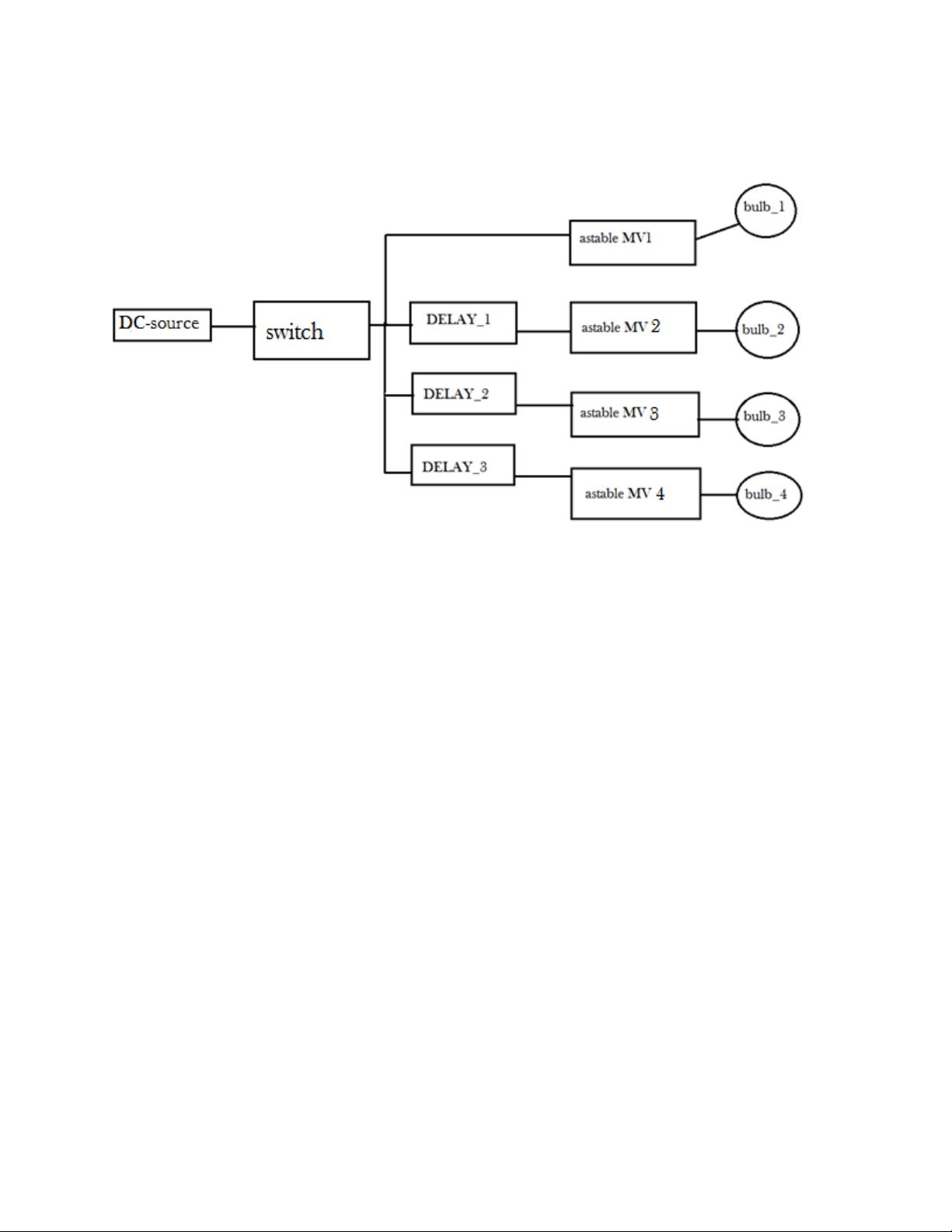
Fig1. Block diagram of the circuit
1. Simple Delay ON Timer Circuit
Simple delay ON timer circuit allows the connected load at the output to be switched ON with
some predetermined delay after power switch ON. The following circuit can be used for all
applications which calls for an initial delay ON feature for the connected load after the main
power is switched ON.
1.1. How does it work
The shown diagram is pretty straightforward yet provides the necessary actions very impressively,
moreover the delay period is variable making the set up extremely useful for the proposed applications.
The functioning can be understood with the following points:
Assuming the load which requires the delay ON action being connected across the relay
contacts, when power is switched ON, the 12V DC passes via R2 but is unable to reach the base
of T1 because initially, C2 acts as a short across ground.
The voltage thus passes through R2, gets dropped to relevant limits and starts charging C2.


