2000 Packaging Databook
14-17
Ball Grid Array (BGA) Packaging
exposure. Maintaining proper control of moisture uptake in components is critical to the prevention
of "popcorning" of the package body or encapsulation material. BGA components, before shipping,
are baked dry and enclosed in a sealed desiccant bag with a desiccant pouch and a humidity indicator
card. Most BGA components are classified as a level 3 or level 4 for moisture sensitivity as per the
IPC/JEDEC Spec J-STD-020, “Moisture/Reflow Sensitivity Calculation of Plastic Surface Mount
Devices.”
With most surface mount components, if the units are allowed to absorb moisture beyond their out
of bag times for their moisture rating, damage may occur during the reflow process. Chapter 8 of
this data book provides an in-depth view of package preconditioning methods and moisture sensi-
tivity requirements. Please refer to Chapter 8 for more information regarding how moisture sensitive
components are classified.
Prior to opening the shipping bag and attempting solder reflow, the moisture sensitivity of the pack-
ages being used should be understood so proper precautions can be taken to insure that a minimal
out of bag time is maintained. This will insure that the highest possible package reliability is
achieved for the final product. If previously bagged product cannot be mounted before the elapsed
out of bag time for that product, the parts can be rebaked as per Chapter 8. Another option is to store
the opened units in a nitrogen cabinet or dry box until needed. Placing units in a dry box effectively
‘stops the clock.’
It should be understood that packages continue to gain moisture even after board mounting. Com-
ponents that need to be reworked must be completely processed throught all thermal exposures be-
fore the original out of bag limits are reached. If this is not possible, or the time allotment is not
ridgely followed, bake-out of the completed boards must be accompliished before subjecting the
components to the heat of the rework process. Products being removed from boards that have been
returned from the field for failure analysis, must be baked dry before heat expousure. If this step is
skipped, massive damage to the component will result, rendering useless any further efforts at de-
termining the cause of failure.
14.8 Designing Boards For BGAs
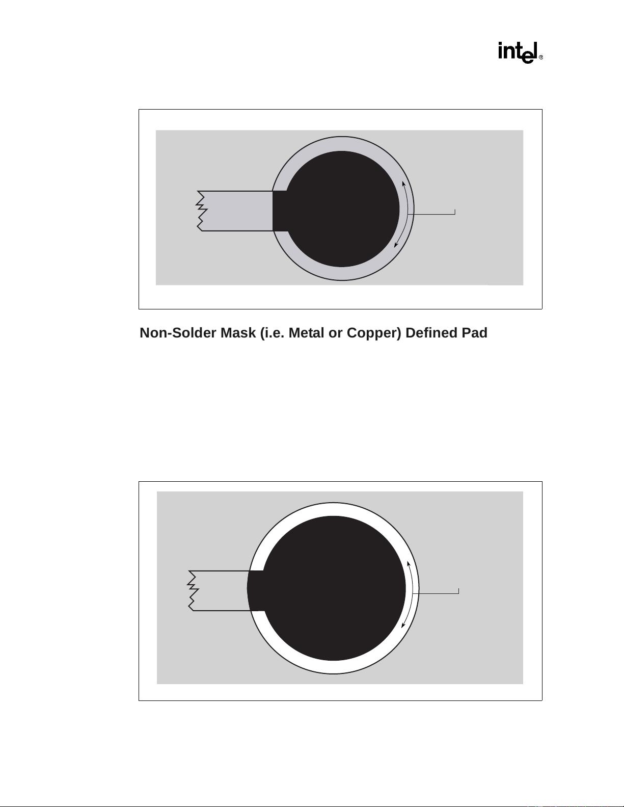
Most BGA packages use Solder Mask Defined pads on the package side of the solder ball. PCB pad
size is typically close to or identical to the package pad size. This provides for balanced stress during
thermal cycling, which helps to maximize fatigue life.
14.8.1 Solder Mask Defined (SMD) Pad
In the solder mask defined (SMD) pad shown in Figure 14-14, the copper for the pad area is larger
than the desired land size. The opening in the solder mask is made smaller than the copper land, thus
defining the mounting pad. A couple of points to consider with solder mask defined pad are:
• There is an advantage in that the overlap of the solder mask onto the copper enhances the
copper adhesion to the laminate surface. When using resin systems where adhesion is low, this
is an important consideration.
• One disadvanatage of SMD pads is that the fatigue life has shown to be lower then NSMD
pads through long term reliaiblity testing. Because of this issue, the solder mask angle at the
pad edge has been thinned on many new package designs to minimize the mask impingment
on the solder ball.