


QPSK Demodulation:
Block Diagram:
Block diagram of QPSK Transmitter b1(t) + QPSK signal I/P binary b (t) Wave Ø1 (t)
= √2/ Tb cos 2πƒct + b2 (t) Ø2 (t) = √2/ Tb sin 2πƒct QPSK Transmitter Block
Diagram The i/p binary sequence b(t) is represented in polar from with symbols 1 & 0
represented as +√E/2 and -√E/2 .This binary wave is demultiplexed into two separate
binary waves consisting of odd & even numbered I/P bits denoted by b1(t) & b2 (t) b1
(t) & b2(t) are used to modulate a pair of quadrature carrier or orthogonal Basis
function Ø1 (t) & Ø2 (t). The result is two PSK waves’ .
These two binary PSK waves are added to produce the desired QPSK signal . QPSK
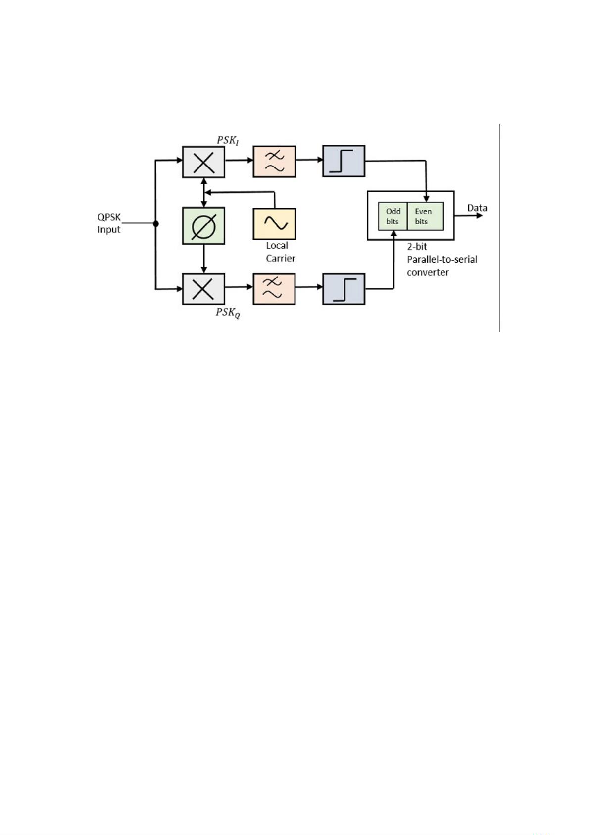
Receiver: QPSK Receiver Block Diagram QPSK receiver consists of a pair of
correlators with common I/P & supplied with Locally generated Signal Ø1 (t) & Ø2
(t).The correlator O/P, x1, & x2 are each compared with a threshold of zero volts.If x1
> 0, decision is made in favour of symbol ‘1’ for upper channel and if x1 > 0, decision
is made in favour of symbol 0. Parallely Y x2 >0, decision is made in favour of
symbol 1 for lower channel & if x2 <0, decision is made in favour of symbol 0. These
two channels are combined in a multiplexer to get the original binary output.
ALGORITHM QPSK Modulation
1.Generate two carrier signals (Ø1 (t) = √2/Tb cos 2πƒct and Ø2 (t) = √2/Tb
cos2πƒct)
2.Generate the base band data signal .
3.Binary wave is divided into odd(b1(t)) and even(b2(t)) numbered input
bits.
4.Multiply the odd numbered data signal (b1(t)) and carrier signal 1 in one
channel .
5..Multiply the even numbered data signal b2 (t)and carrier signal 2in
another channel
6.Sum the output resultant signals of step 4 and 5.


