2001 Microchip Technology Inc. DS35007B
PIC16F84A
Data Sheet
18-pin Enhanced FLASH/EEPROM
8-bit Microcontroller
M

DS35007B - page ii 2001 Microchip Technology Inc.
Information contained in this publication regarding device
applications and the like is intended through suggestion only
and may be superseded by updates. It is your responsibility to
ensure that your application meets with your specifications.
No representation or warranty is given and no liability is
assumed by Microchip Technology Incorporated with respect
to the accuracy or use of such information, or infringement of
patents or other intellectual property rights arising from such
use or otherwise. Use of Microchip’s products as critical com-
ponents in life support systems is not authorized except with
express written approval by Microchip. No licenses are con-
veyed, implicitly or otherwise, under any intellectual property
rights.
Trademarks
The Microchip name and logo, the Microchip logo, PIC, PICmicro,
PICMASTER, PICSTART, PRO MATE, K
EELOQ, SEEVAL,
MPLAB and The Embedded Control Solutions Company are reg-
istered trademarks of Microchip Technology Incorporated in the
U.S.A. and other countries.
Total Endurance, ICSP, In-Circuit Serial Programming, Filter-
Lab, MXDEV, microID,
Flex
ROM,
fuzzy
LAB, MPASM,
MPLINK, MPLIB, PICC, PICDEM, PICDEM.net, ICEPIC,
Migratable Memory, FanSense, ECONOMONITOR, Select
Mode and microPort are trademarks of Microchip Technology
Incorporated in the U.S.A.
Serialized Quick Term Programming (SQTP) is a service mark
of Microchip Technology Incorporated in the U.S.A.
All other trademarks mentioned herein are property of their
respective companies.
© 2001, Microchip Technology Incorporated, Printed in the
U.S.A., All Rights Reserved.
Printed on recycled paper.
Microchip received QS-9000 quality system
certification for its worldwide headquarters,
design and wafer fabrication facilities in
Chandler and Tempe, Arizona in July 1999. The
Company’s quality system processes and
procedures are QS-9000 compliant for its
PICmicro
®
8-bit MCUs, KEELOQ
®
code hopping
devices, Serial EEPROMs and microperipheral
products. In addition, Microchip’s quality
system for the design and manufacture of
development systems is ISO 9001 certified.
Note the following details of the code protection feature on PICmicro
®
MCUs.
• The PICmicro family meets the specifications contained in the Microchip Data Sheet.
• Microchip believes that its family of PICmicro microcontrollers is one of the most secure products of its kind on the market today,
when used in the intended manner and under normal conditions.
• There are dishonest and possibly illegal methods used to breach the code protection feature. All of these methods, to our knowl-
edge, require using the PICmicro microcontroller in a manner outside the operating specifications contained in the data sheet.
The person doing so may be engaged in theft of intellectual property.
• Microchip is willing to work with the customer who is concerned about the integrity of their code.
• Neither Microchip nor any other semiconductor manufacturer can guarantee the security of their code. Code protection does not
mean that we are guaranteeing the product as “unbreakable”.
• Code protection is constantly evolving. We at Microchip are committed to continuously improving the code protection features of
our product.
If you have any further questions about this matter, please contact the local sales office nearest to you.

2001 Microchip Technology Inc. DS35007B-page 1
M
PIC16F84A
High Performance RISC CPU Features:
• Only 35 single word instructions to learn
• All instructions single-cycle except for program
branches which are two-cycle
• Operating speed: DC - 20 MHz clock input
DC - 200 ns instruction cycle
• 1024 words of program memory
• 68 bytes of Data RAM
• 64 bytes of Data EEPROM
• 14-bit wide instruction words
• 8-bit wide data bytes
• 15 Special Function Hardware registers
• Eight-level deep hardware stack
• Direct, indirect and relative addressing modes
• Four interrupt sources:
- External RB0/INT pin
- TMR0 timer overflow
- PORTB<7:4> interrupt-on-change
- Data EEPROM write complete
Peripheral Features:
• 13 I/O pins with individual direction control
• High current sink/source for direct LED drive
- 25 mA sink max. per pin
- 25 mA source max. per pin
• TMR0: 8-bit timer/counter with 8-bit
programmable prescaler
Special Microcontroller Features:
• 10,000 erase/write cycles
Enhanced
FLASH
Program memory typical
• 10,000,000 typical erase/write cycles EEPROM
Data memory typical
• EEPROM Data Retention > 40 years
• In-Circuit Serial Programming™ (ICSP™) - via
two pins
• Power-on Reset (POR), Power-up Timer (PWRT),
Oscillator Start-up Timer (OST)
• Watchdog Timer (WDT) with its own On-Chip RC
Oscillator for reliable operation
• Code protection
• Power saving SLEEP mode
• Selectable oscillator options
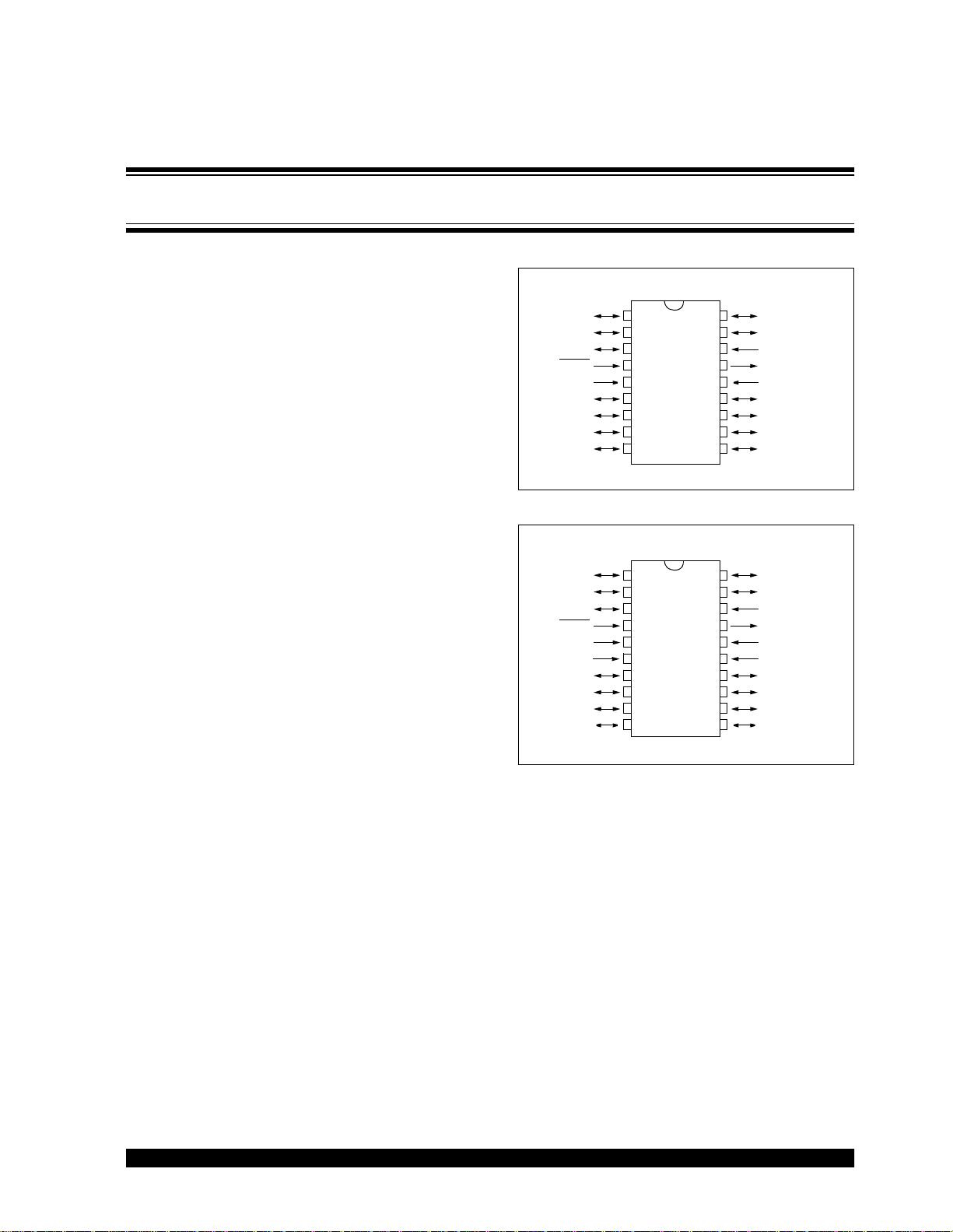
Pin Diagrams
CMOS Enhanced
FLASH/EEPROM
Technology:
• Low power, high speed technology
• Fully static design
• Wide operating voltage range:
- Commercial: 2.0V to 5.5V
- Industrial: 2.0V to 5.5V
• Low power consumption:
- < 2 mA typical @ 5V, 4 MHz
-15 µA typical @ 2V, 32 kHz
- < 0.5 µA typical standby current @ 2V
RA1
RA0
OSC1/CLKIN
OSC2/CLKOUT
V
DD
RB7
RB6
RB5
RB4
RA2
RA3
RA4/T0CKI
MCLR
VSS
RB0/INT
RB1
RB2
RB3
•
1
2
3
4
5
6
7
8
9
18
17
16
15
14
13
12
11
10
PDIP, SOIC
PIC16F84A
RA1
RA0
OSC1/CLKIN
OSC2/CLKOUT
V
DD
RB7
RB6
RB5
RB4
RA2
RA3
RA4/T0CKI
MCLR
VSS
RB0/INT
RB1
RB2
RB3
•
1
2
3
4
5
6
7
8
9
20
19
18
17
16
15
14
13
12
SSOP
PIC16F84A
10
11
VSS
VDD
18-pin Enhanced FLASH/EEPROM 8-Bit Microcontroller

PIC16F84A
DS35007B-page 2 2001 Microchip Technology Inc.
Table of Contents
1.0 Device Overview .......................................................................................................................................................................... 3
2.0 Memory Organization................................................................................................................................................................... 5
3.0 Data EEPROM Memory ............................................................................................................................................................. 13
4.0 I/O Ports ..................................................................................................................................................................................... 15
5.0 Timer0 Module ........................................................................................................................................................................... 19
6.0 Special Features of the CPU...................................................................................................................................................... 21
7.0 Instruction Set Summary ............................................................................................................................................................ 35
8.0 Development Support................................................................................................................................................................. 43
9.0 Electrical Characteristics............................................................................................................................................................ 49
10.0 DC/AC Characteristic Graphs .................................................................................................................................................... 61
11.0 Packaging Information................................................................................................................................................................ 71
Appendix A: Revision History .............................................................................................................................................................. 75
Appendix B: Conversion Considerations.............................................................................................................................................. 76
Appendix C: Migration from Baseline to Mid-Range Devices .............................................................................................................. 78
Index .................................................................................................................................................................................................... 79
On-Line Support................................................................................................................................................................................... 83
Reader Response ................................................................................................................................................................................ 84
PIC16F84A Product Identification System........................................................................................................................................... 85
TO OUR VALUED CUSTOMERS
It is our intention to provide our valued customers with the best documentation possible to ensure successful use of your Microchip
products. To this end, we will continue to improve our publications to better suit your needs. Our publications will be refined and
enhanced as new volumes and updates are introduced.
If you have any questions or comments regarding this publication, please contact the Marketing Communications Department via
E-mail at docerrors@mail.microchip.com or fax the Reader Response Form in the back of this data sheet to (480) 792-4150.
We welcome your feedback.
Most Current Data Sheet
To obtain the most up-to-date version of this data sheet, please register at our Worldwide Web site at:
http://www.microchip.com
You can determine the version of a data sheet by examining its literature number found on the bottom outside corner of any page.
The last character of the literature number is the version number, (e.g., DS30000A is version A of document DS30000).
Errata
An errata sheet, describing minor operational differences from the data sheet and recommended workarounds, may exist for current
devices. As device/documentation issues become known to us, we will publish an errata sheet. The errata will specify the revision
of silicon and revision of document to which it applies.
To determine if an errata sheet exists for a particular device, please check with one of the following:
• Microchip’s Worldwide Web site; http://www.microchip.com
• Your local Microchip sales office (see last page)
• The Microchip Corporate Literature Center; U.S. FAX: (480) 792-7277
When contacting a sales office or the literature center, please specify which device, revision of silicon and data sheet (include liter-
ature number) you are using.
Customer Notification System
Register on our web site at www.microchip.com/cn to receive the most current information on all of our products.

2001 Microchip Technology Inc. DS35007B-page 3
PIC16F84A
1.0 DEVICE OVERVIEW
This document contains device specific information for
the operation of the PIC16F84A device. Additional
information may be found in the PICmicro™ Mid-
Range Reference Manual, (DS33023), which may be
downloaded from the Microchip website. The Refer-
ence Manual should be considered a complementary
document to this data sheet, and is highly recom-
mended reading for a better understanding of the
device architecture and operation of the peripheral
modules.
The PIC16F84A belongs to the mid-range family of the
PICmicro
®
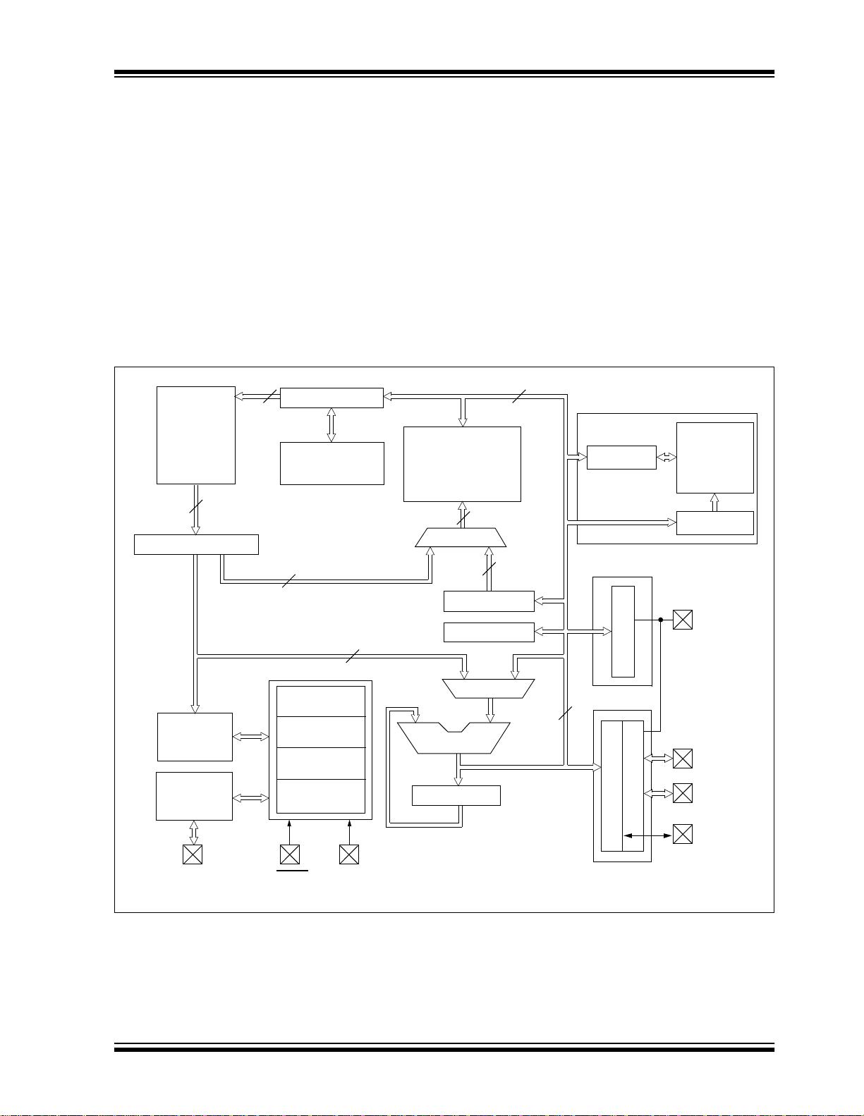
microcontroller devices. A block diagram of
the device is shown in Figure 1-1.
The program memory contains 1K words, which trans-
lates to 1024 instructions, since each 14-bit program
memory word is the same width as each device instruc-
tion. The data memory (RAM) contains 68 bytes. Data
EEPROM is 64 bytes.
There are also 13 I/O pins that are user-configured on
a pin-to-pin basis. Some pins are multiplexed with other
device functions. These functions include:
• External interrupt
• Change on PORTB interrupt
• Timer0 clock input
Table 1-1 details the pinout of the device with descrip-
tions and details for each pin.
FIGURE 1-1: PIC16F84A BLOCK DIAGRAM
FLASH
Program
Memory
Program Counter
13
Program
Bus
Instruction Register
8 Level Stack
(13-bit)
Direct Addr
8
Instruction
Decode &
Control
Timing
Generation
OSC2/CLKOUT
OSC1/CLKIN
Power-up
Timer
Oscillator
Start-up Timer
Power-on
Reset
Watchdog
Timer
MCLR
VDD, VSS
W reg
ALU
MUX
I/O Ports
TMR0
STATUS reg
FSR reg
Indirect
Addr
RA3:RA0
RB7:RB1
RA4/T0CKI
EEADR
EEPROM
Data Memory
64 x 8
EEDATA
Addr Mux
RAM Addr
RAM
File Registers
EEPROM Data Memory
Data Bus
5
7
7
RB0/INT
14
8
8
1K x 14
68 x 8


