


PLL DESIGN AND
CLOCK/FREQUENCY GENERATION
(Lecture 5)
Woogeun Rhee
Institute of Microelectronics
Tsinghua University
Spring Semester, 2011

2
W. Rhee, Institute of Microelectronics, Tsinghua University
III. PLL Design
1. Circuit Design Aspects
B. Charge pump
3
W. Rhee, Institute of Microelectronics, Tsinghua University
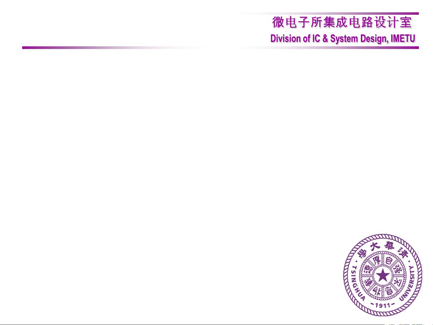
Circuit Design – Charge Pump
• CP is the block which converts phase information (time domain)
into analog quantity (voltage domain).
• CP design is critical especially when division ratio is high.
K
d
= I
CP
R/2p
v
p
q
2p
-2p
4p
I
CP
R
with Z(s) R
A
B
PFD
U
D
I
CP
Z(s)
A
B
U
D
I
CP

4
W. Rhee, Institute of Microelectronics, Tsinghua University
Charge Pump Design Consideration
• Understanding deadzone effect on PLL
• Operating frequency
- Differential design for high frequency operation
• Noise
- CP noise becomes critical with high division ratio.
• Leakage current
- High CP current needed.
- Differential design more immune to leakage current.
• Mismatch
- Minimized with fully differential design.
• Switching noise
- Minimized with fully differential design.
• Charge sharing with LPF
- Can be reduced by feedback circuit
• Linearity
- High timing resolution improves linearity.
5
W. Rhee, Institute of Microelectronics, Tsinghua University
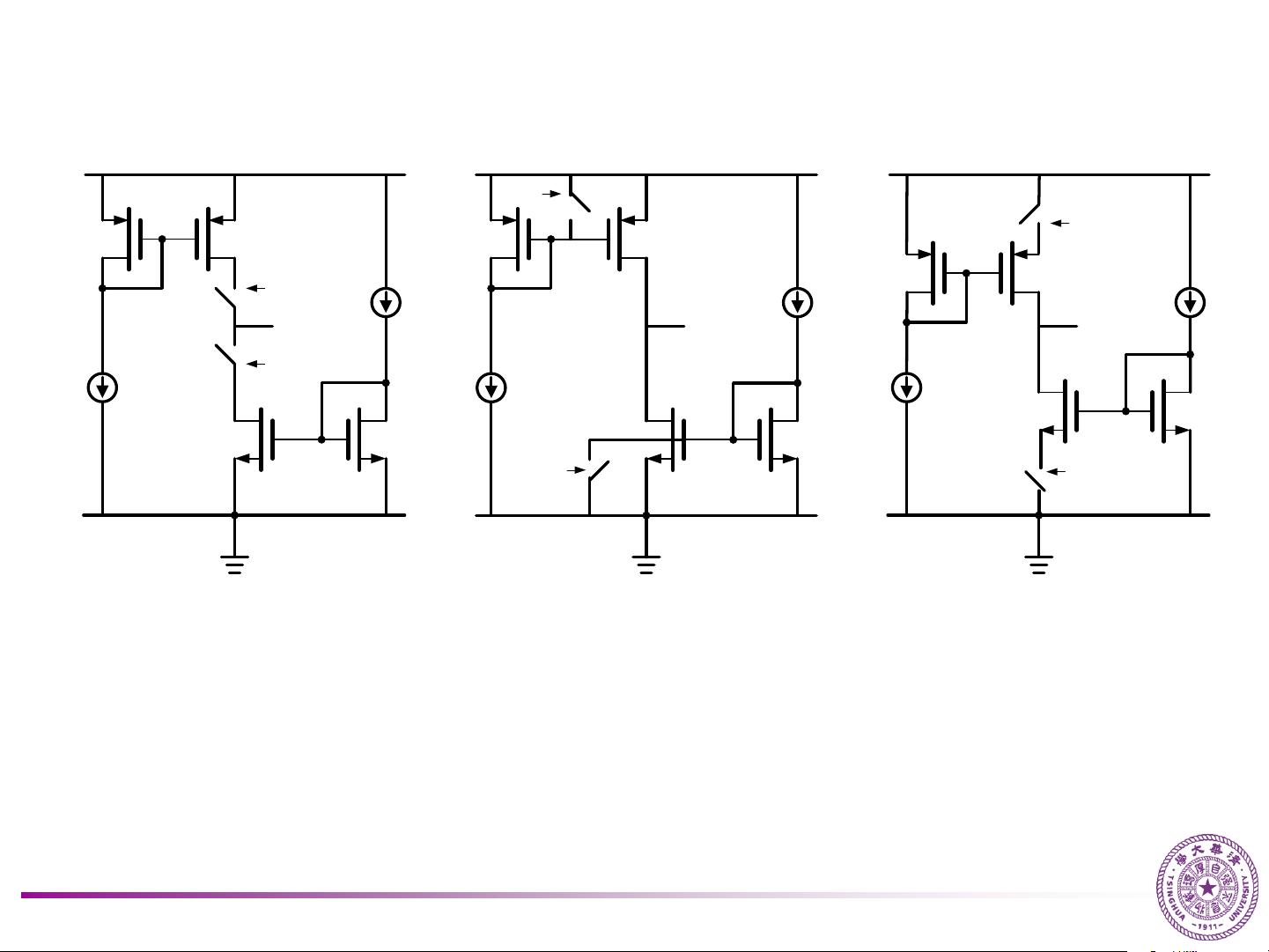
M1
M2
M3
M4
IUP
IDW
OUT
UP
DW
Topology – Single-Ended
• Generates high peak current during switching (a)
• Requires low (W/L)
3
/(W/L)
1
for fast switching (b)
• Less sensitive to gate capacitance but longer turn-off time (c)
M1
M2
M3
M4
IUP
IDW
OUT
DW
UP
(a) (b) (c)
M1
M2
M3
M4
IUP
IDW
UP
DW
OUT


