

Computer Science 152: Laboratory 7-Final Project Kelford, Lai, Mao, Yeh
December 12, 2001
Section 102: M 2-4
Laboratory 7
Final Project: Multi-processing, Secondary-cache,
Write-buffer
By
Brett Kelford
Kevin Lai
Helen Mao
David Yeh
Control Freaks
December 12, 2001
Section 102: Mon. 2-4 Ed Liao
Computer Science 152: Laboratory 7-Final Project Kelford, Lai, Mao, Yeh
December 12, 2001
Section 102: M 2-4
Abstract
The purpose of this project is to explore the issues and implementation of a multiple instruction
stream, single data stream processor. We are running two instruction streams on two CPUs
which share an address space. The processors share a second level cache, and maintain
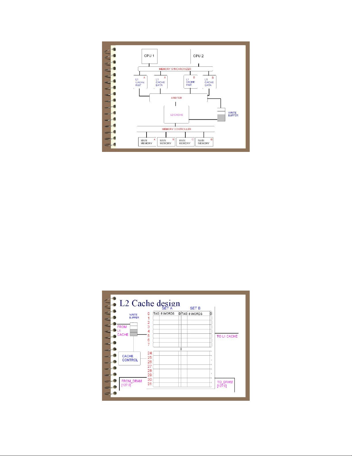
coherence at the L1 cache with a write-invalidate policy. The L2 cache is two-way set associative,
with a block size of 8 words, and a total capacity of 512 words. The L2 cache is connected to a
DRAM system by a 128-bit bus to alleviate cache miss penalties. Writes are done directly to the
L2 level (writeback to L2), where a write buffer improves write performance. Synchronization
variables are implemented by intercepting loads and stores to the address space that represents
the sync variables, and performing atomic operations that provide lock functionality.
Division of labor
These things needed to be done for the project.
1) Synchronization mechanism, synchronization variables
2) Cache coherence at the L1 level – Write invalidate policy.
3) Write buffer
4) L2 cache schematic
5) L2 cache controller
6) Memory controller changes for writeback policy, interface with L2 cache, and 128-bit bus.
7) Instruction monitor for two instruction streams.
8) Arbiter changes.
9) Putting together all the components.
10) Testing.
Each component is tested individually by the responsible person for basic functionality, then we
ran tests on the combined system.
Brett Kelford
Synchronization variables, multiple process stream monitor, arbitration.
Kevin Lai
L2 cache schematic, Presentation out-line, write-up
Helen Mao
L2 cache controller, Memory controller for 4 DRAM, L2 cache schematic,
Write invalidates to the L1 cache, testing.
David Yeh
Write buffer, testing, write-up
Detailed Strategy
Our strategy was guided by three goals: correctness, quickness of implementation, and speed of
processor.
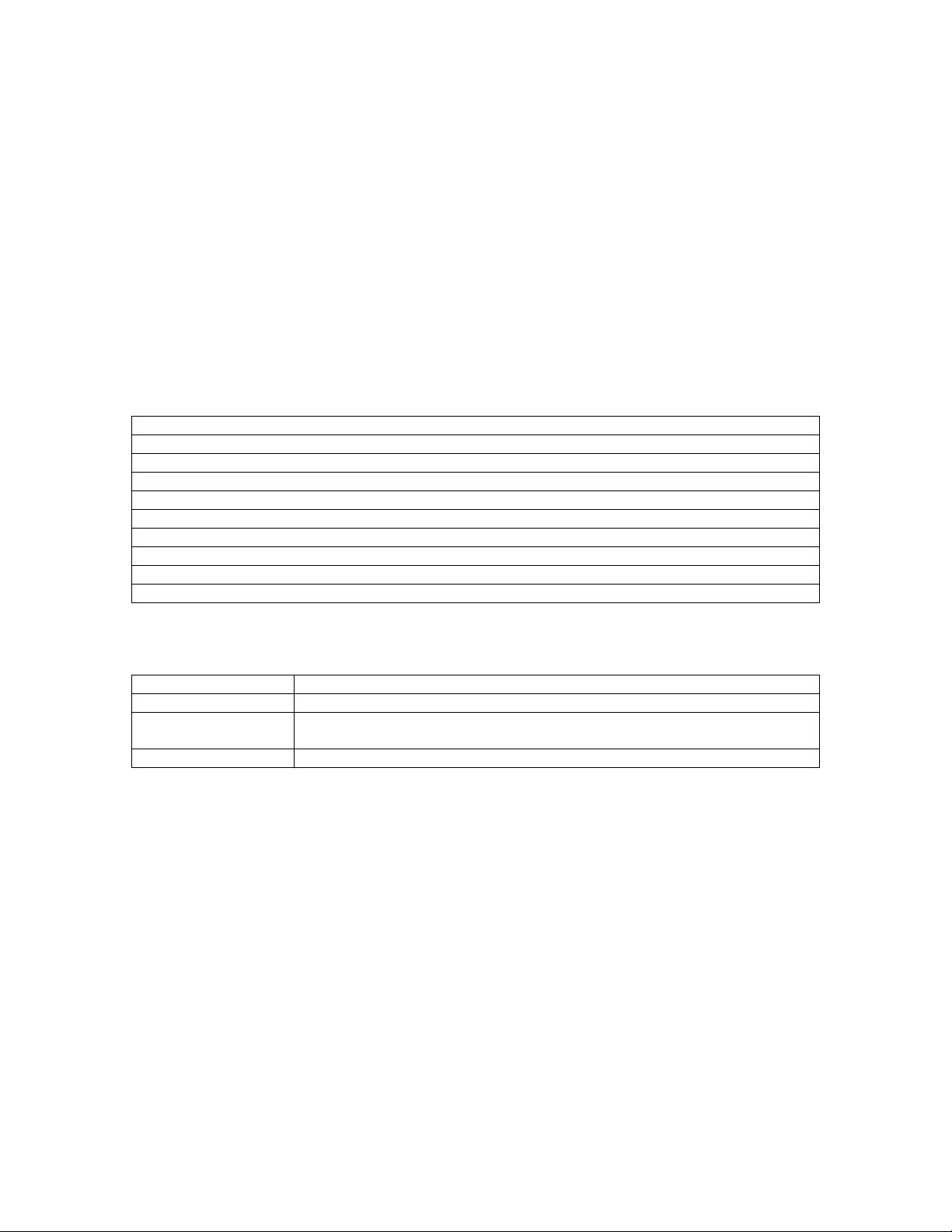
Our top-level design can be summarized into the following:
� Two CPUs synchronized using a memory synchronizer
� 4 L1 caches (2 Data and 2 Instructional) that use a single L2 cache through an arbiter. It
uses write-through policy in relation to the L2 cache, in much the same way it originally
did for memory in our previous lab.
� A write-buffer for writes from the L1 to the L2 caches
� A memory controller that allows the L2 cache to access 4 interleaving memories. The L2
cache uses a write-back policy and maintains a dirty bit.
Computer Science 152: Laboratory 7-Final Project Kelford, Lai, Mao, Yeh
December 12, 2001
Section 102: M 2-4
L2 cache system
A shared L2 cache allows a single memory space to be shared between multiple processors. An
arbiter allows only one component to access the L2 cache at a time. Increasing the number of
ports to the system could make the system faster by allowing parallel reads and writes, but that
seemed too difficult to implement in two weeks’ time to justify improving the miss penalty of
accesses that miss the L1 and hit the L2. This choice only significantly affects programs with a
high L1 miss rate.
To improve the miss penalty of the L2 cache, we implemented the maximum allowable DRAM
bus size of 128-bits. Since the L2 cache block size is 8 words, frequent misses to the L2 will
actually slow down processor performance because it would require reading 8 words rather than
the one that actually needs to be used. Reading four words in parallel alleviates this penalty by
bringing the miss time closer to that of a single word access.
Since L2 misses are so costly, in part because of the 8 word block size, we decided to improve
the miss rate of the L2 cache by implementing a 2-way L2 cache with LRU replacement policy. A
2-way cache reduces conflict misses to equal approximately that of a cache twice its size. We
chose the LRU policy because for a 2-way cache it is not harder to implement than random block
replacement and makes testing more predictable.