soiseek
搜
iC
世界首个完全基于中文的IC专业搜索引擎。立即访问Soiseek 搜索中文Datasheet!
IC搜索 手气不错
上 www.soiseek.cn 看中文版IC手册!
小提示:使用空格同时搜索多个关键词。尝试“atmel 8 bit 微控制器”。
世界首个 全中文IC搜索引擎
IC型号大全 - 关于Soiseek - 发送反馈
把Soiseek设为首页
版权声明:
Soiseek所提供的所有IC数据手册(Datasheet)的中文译本,仅供参考,所有版权归发布厂商所有。
对于可能出现的翻译错误,Soiseek恕不负责。请用户以原版数据手册内容为准。
Soiseek免费提供下载的IC数据手册(Datasheet)的PDF来自于发布厂商,所有版权归发布厂商所有。
Soiseek不对数据手册(Datasheet)中内容的真实性和准确性负责。
欢迎提出建议,指正错误与疏漏。我们永远致力于为您提供更好的搜索结果。
联系我们:http://www.soiseek.cn/tellus

©2006 Silicon Storage Technology, Inc.
S71233-05-000 1/06
1
The SST logo and SuperFlash are registered trademarks of Silicon Storage Technology, Inc.
These specifications are subject to change without notice.
Data Sheet
FEATURES:
• Single 2.7-3.6V Read and Write Operations
• Serial Interface Architecture
– SPI Compatible: Mode 0 and Mode 3
• 20 MHz Max Clock Frequency
• Superior Reliability
– Endurance: 100,000 Cycles (typical)
– Greater than 100 years Data Retention
• Low Power Consumption:
– Active Read Current: 7 mA (typical)
– Standby Current: 8 µA (typical)
• Flexible Erase Capability
– Uniform 4 KByte sectors
– Uniform 32 KByte overlay blocks
• Fast Erase and Byte-Program:
– Chip-Erase Time: 70 ms (typical)
– Sector- or Block-Erase Time: 18 ms (typical)
– Byte-Program Time: 14 µs (typical)
• Auto Address Increment (AAI) Programming
– Decrease total chip programming time over
Byte-Program operations
• End-of-Write Detection
– Software Status
• Hold Pin (HOLD#)
– Suspends a serial sequence to the memory
without deselecting the device
• Write Protection (WP#)
– Enables/Disables the Lock-Down function of the
status register
• Software Write Protection
– Write protection through Block-Protection bits in
status register
• Packages Available
– 8-lead SOIC (4.9mm x 6mm)
– 8-contact WSON
• All non-Pb (lead-free) devices are RoHS compliant
PRODUCT DESCRIPTION
SST’s serial flash family features a four-wire, SPI-com-
patible interface that allows for a low pin-count package
occupying less board space and ultimately lowering total
system costs. SST25VF010 SPI serial flash memory is
manufactured with SST’s proprietary, high performance
CMOS SuperFlash Technology. The split-gate cell design
and thick-oxide tunneling injector attain better reliability
and manufacturability compared with alternate
approaches.
The SST25VF010 device significantly improves perfor-
mance, while lowering power consumption. The total
energy consumed is a function of the applied voltage,
current, and time of application. Since for any given volt-
age range, the SuperFlash technology uses less current
to program and has a shorter erase time, the total energy
consumed during any Erase or Program operation is less
than alternative flash memory technologies. The
SST25VF010 device operates with a single 2.7-3.6V
power supply.
The SST25VF010 device is offered in both 8-lead SOIC
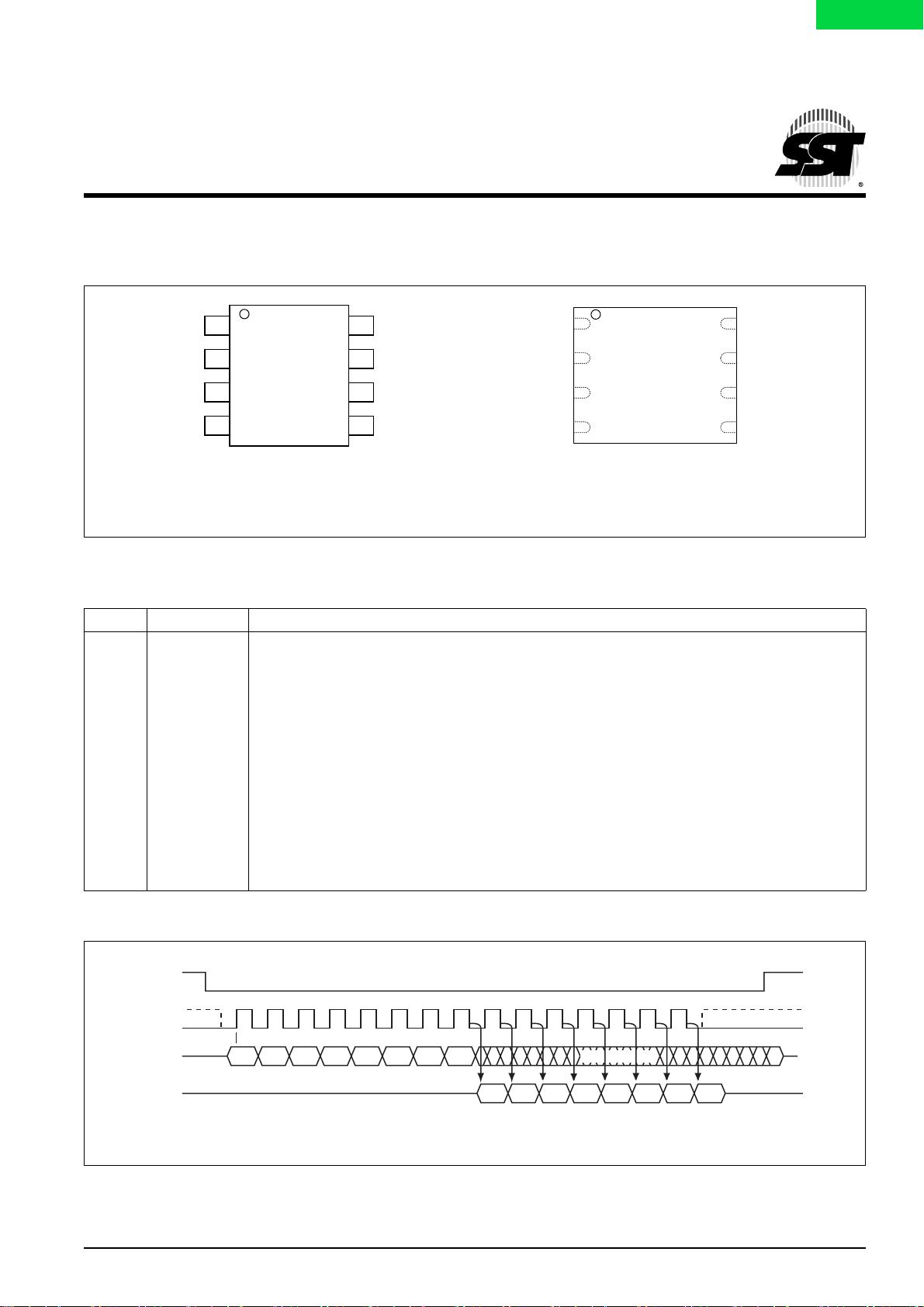
and 8-contact WSON packages. See Figure 1 for the pin
assignments.
1 Mbit SPI Serial Flash
SST25VF010
SST25VF0101Mb Serial Peripheral Interface (SPI) flash memory
soiseek.cn

Data Sheet
1 Mbit SPI Serial Flash
SST25VF010
3
©2006 Silicon Storage Technology, Inc. S71233-05-000 1/06
PIN DESCRIPTION
FIGURE 1: PIN ASSIGNMENTS
FIGURE 2: SPI PROTOCOL
TABLE 1: PIN DESCRIPTION
Symbol Pin Name Functions
SCK Serial Clock To provide the timing of the serial interface.
Commands, addresses, or input data are latched on the rising edge of the clock input, while output
data is shifted out on the falling edge of the clock input.
SI Serial Data
Input
To transfer commands, addresses, or data serially into the device.
Inputs are latched on the rising edge of the serial clock.
SO Serial Data
Output
To transfer data serially out of the device.
Data is shifted out on the falling edge of the serial clock.
CE# Chip Enable The device is enabled by a high to low transition on CE#. CE# must remain low for the duration of
any command sequence.
WP# Write Protect The Write Protect (WP#) pin is used to enable/disable BPL bit in the status register.
HOLD# Hold To temporarily stop serial communication with SPI flash memory without resetting the device.
V
DD
Power Supply To provide power supply (2.7-3.6V).
V
SS
Ground
T1.0 1233
1
2
3
4
8
7
6
5
CE#
SO
WP#
V
SS
V
DD
HOLD#
SCK
SI
Top View
1233 08-soic P1.0
8-LEAD SOIC 8-CONTACT WSON
1
2
3
4
8
7
6
5
CE#
SO
WP#
V
SS
Top View
V
DD
HOLD#
SCK
SI
1233 08-wson P2.0
1233 F02.1
MODE 3
SCK
SI
SO
CE#
MODE 3
DON'T CARE
Bit 7 Bit 6 Bit 5 Bit 4 Bit 3 Bit 2 Bit 1 Bit 0
Bit 7 Bit 6 Bit 5 Bit 4 Bit 3 Bit 2 Bit 1 Bit 0
MODE 0MODE 0
HIGH IMPEDANCE
MSB
MSB
soiseek.cn

4
Data Sheet
1 Mbit SPI Serial Flash
SST25VF010
©2006 Silicon Storage Technology, Inc. S71233-05-000 1/06
PRODUCT IDENTIFICATION
MEMORY ORGANIZATION
The SST25VF010 SuperFlash memory array is organized
in 4 KByte sectors with 32 KByte overlay blocks.
DEVICE OPERATION
The SST25VF010 is accessed through the SPI (Serial
Peripheral Interface) bus compatible protocol. The SPI bus
consist of four control lines; Chip Enable (CE#) is used to
select the device, and data is accessed through the Serial
Data Input (SI), Serial Data Output (SO), and Serial Clock
(SCK).
The SST25VF010 supports both Mode 0 (0,0) and Mode 3
(1,1) of SPI bus operations. The difference between the
two modes, as shown in Figure 2, is the state of the SCK
signal when the bus master is in Stand-by mode and no
data is being transferred. The SCK signal is low for Mode 0
and SCK signal is high for Mode 3. For both modes, the
Serial Data In (SI) is sampled at the rising edge of the SCK
clock signal and the Serial Data Output (SO) is driven after
the falling edge of the SCK clock signal.
TABLE 2: P
RODUCT IDENTIFICATION
Address Data
Manufacturer’s ID 00000H BFH
Device ID
SST25VF010 00001H 49H
T2.0 1233
soiseek.cn


