


AN10897
A guide to designing for ESD and EMC
Rev. 02 — 19 January 2010 Application note
Document information
Info Content
Keywords ESD, EMC, PCB design
Abstract An introductory approach to designing for ESD. Understanding the ESD
pulse, how passive components react over frequency, and PCB layout
techniques are exposed.

AN10897_2 © NXP B.V. 2010. All rights reserved.
Application note Rev. 02 — 19 January 2010 2 of 30
Contact information
For more information, please visit: http://www.nxp.com
For sales office addresses, please send an email to: [email protected]
NXP Semiconductors
AN10897
A guide to designing for ESD and EMC
Revision history
Rev Date Description
02 20100119 application note; second release
Modifications: • Title of application note modified: appended “and EMC”
• Section 2.3.5 “Filters”, 1
st
bullet item, 2
nd
sub-bullet: changed from “high filter capacitors”
to “high speed capacitors”
• Section 2.3.6 “Ground”, 2
nd
equation following 3
rd
paragraph changed from
“V = 20 × 10e−9 × (10A/10e−9)” to “V = 20 nH × (10A/10ns)”
• Section 3.1 “Board structure - functional grouping”: 3
rd
paragraph re-written.
• Section 3.1.1.1 “4-layer board stack-up”, 2
nd
sentence: changed from “use a wide core”
to “use a thick core”.
• Figure 18 “Recommended stack-ups” modified (adjusted height of stack-up layers)
• Section 3.1.2 “Ground planes”:
– deleted 3
rd
and 4
th
bullet items following the 3
rd
paragraph.
– 4
th
paragraph (immediately follows Figure 23) was re-written (now 4
th
, 5
th
and 6
th
paragraphs).
• Figure 26 “Ground island and vias” modified (added label “vias to ground” on left side).
• Figure 31 “Ground plane boundary” modified (added “20 × layer spacing” measurement)
01 20091214 application note; initial version

AN10897_2 © NXP B.V. 2010. All rights reserved.
Application note Rev. 02 — 19 January 2010 3 of 30
NXP Semiconductors
AN10897
A guide to designing for ESD and EMC
1. Introduction
This application note is written to give the user an introductory approach to dealing with
ESD. Be it a Pachinko machine or a washing machine or a hand held remote control, ESD
is a threat to the operation of the system and it needs to be addressed head-on.
Given the nature of the product, it will be exposed to ESD events that range from the
normal charge build-up in human beings using the equipment, charge build-up by moving
parts (due to triboelectric charging), or by malicious attacks by individuals.
It is important to note that this manual is a set of guidelines that will improve the system
immunity to ESD events and that it is not a guarantee that it will prevent an ESD event
from altering the performance of your product or eliminating potential damage.
When it comes to ESD, keep the following quote from Og Mandino in mind: “Never has
there been a map, however carefully executed to detail and scale, which carried its owner
over even one inch of ground.” It is upon you to take action into implementing the
recommendation presented and testing the results of the recommendation in your
application. You must also test for ESD at various points in the design phase to guarantee
performance of the final product.
2. The basics
2.1 The ESD pulse
2.1.1 Characteristics of the ESD pulse—the IEC model
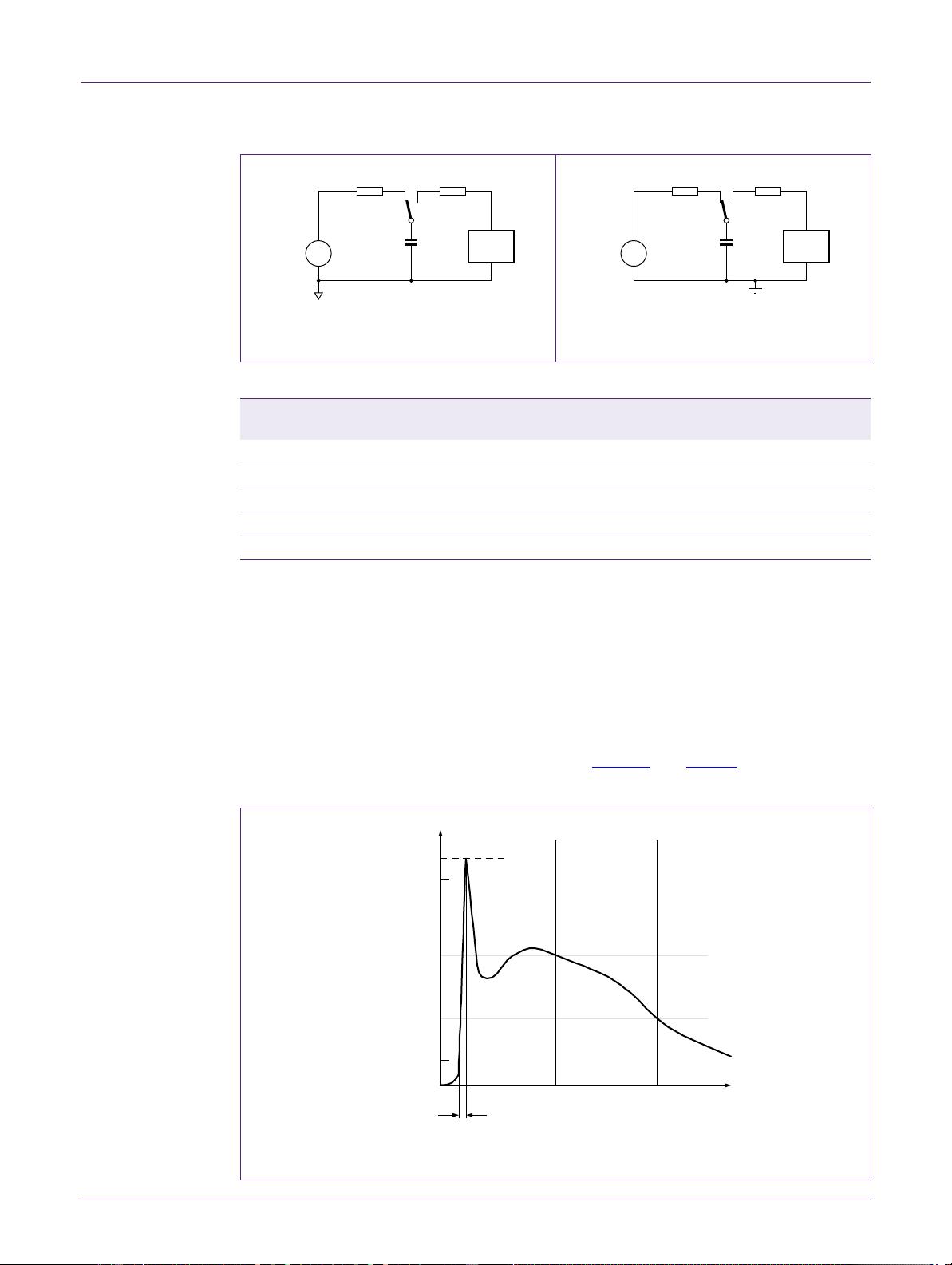
In this guide the ESD pulse we will be referring to is the one defined in IEC 61000-4-2.
The typical test circuit is shown in Figure 1
and the characteristics of the pulse is shown in
Figure 4
.
There are other specifications such as the Human Body Model (HBM) (see Figure 2
for
typical HBM test circuit) and the Machine Model (MM). These models are device level
specifications and are used to qualify IC components and intended for customer assembly
production lines. Device-level ESD pulses (HBM, MM, CDM) and system-level ESD
pulses (IEC) should be considered with separate test acceptance criteria. There is a
disconnect in the EMC (ElectroMagnetic Compatibility) world between system
manufacturers testing systems for upset and device manufacturers testing devices for
failure. Some system level manufacturers are pushing device manufacturers to test
semiconductor devices using system-level compliance standards—specifically,
IEC 61000-4-2 for ESD (ElectroStatic Discharge). Product manufacturers would like to
believe that if devices are qualified to IEC standard(s), finished products will likewise be
qualified. Unfortunately, there is a fundamental difference between system-level and
device-level testing. Table 1
shows a comparison between the peak current of HBM
versus IEC 61000-4-2 standards.
AN10897_2 © NXP B.V. 2010. All rights reserved.
Application note Rev. 02 — 19 January 2010 4 of 30
NXP Semiconductors
AN10897
A guide to designing for ESD and EMC
The human body has the ability to charge and store energy with a charge that can reach
several thousands of volts (8 kV to 10 kV is common) and peak currents from 1 A up to
200 A. The timing in which this charge is delivered varies as follows:
Rise time: t
r
= 200 ps to 20 ns
Spike time: t
spike
= 0.5 ns to 10 ns
Total time: t
tot
= 100 ns to 2 µs
The IEC specification ESD waveform has similar characteristics, however, the amount of
energy delivered is far greater than a HBM pulse. Figure 3
and Table 2 show the current
levels at different time points.
Fig 1. Test circuit according to
IEC 61000-4-2
Fig 2. Typical HBM test circuit
Table 1. Peak current of HBM versus IEC 61000-4-2 ESD standards
Applied voltage (kV) Peak current (A)
Human Body Model
Peak current (A)
IEC 61000-4-2
2 1.33 7.5
42.6715.0
64.0022.5
85.3330.0
10 6.67 37.5
Fig 3. ESD surge according to IEC 61000-4-2
DUT
150 pF
330 Ω
50 MΩ to 100 MΩ
V
V
gen
high-voltage
generator
002aae87
0
DUT
100 pF
1.5 kΩ
1 MΩ
V
V
gen
high supply
voltage
002aaf15
3
time
60 ns
30 ns
100 %
90 %
10 %
I
peak
at 60 ns
I
peak
at 30 ns
002aae871
I
peak
t
r
= 0.7 ns to 1 ns

AN10897_2 © NXP B.V. 2010. All rights reserved.
Application note Rev. 02 — 19 January 2010 5 of 30
NXP Semiconductors
AN10897
A guide to designing for ESD and EMC
The IEC-61000-4-2 also specifies compliance levels, with a Level 4 being the most severe
and representing a 8 kV contact discharge or a 15 kV air discharge onto the Equipment
Under Test (EUT).
When a discharge into equipment occurs, the discharge current will flow through the
equipment through different paths. The high frequency components will flow radially,
whereas the low frequency components will seek the path of least resistance to ground.
This current flow will excite any existing antennas (antennas are described later) in their
path. The efficiency (gain) of these antennas are primarily dependent on their size. Since
a
1
⁄
4
wave length antenna is very efficient, it can easily have a dimension of 1.5 cm to
150 m. For ESD events, even a
1
⁄
20
wave length antenna may conduct a significant
amount of energy.
2.1.2 Putting the ESD problem into perspective
We will model an ESD pulse with a simple circuit:
V1 = voltage source
R2 = generator source resistance
C1 = capacitance A
R1 = load resistance
Table 2. IEC 61000-4-2 ESD surge classification
1a - Contact discharge 1b - Air discharge
Class Test voltage (kV) Maximum current (A) Class Test voltage (kV)
12 7.5 12
24 15 24
36 22.5 38
48 30 415
X special special X special
(1) NoiseKEN output coupling capacitor and 300 Ω source resistance
Fig 4. ESD pulse model
C1
150 pF
R1
1 Ω
R2
(1)
300 Ω
4
8
0
12
16
−4
440 620500
V
i
V
o
V1
560
V
i
(kV)
time (ns)


