通力561主板电路原理图
需积分: 5 70 浏览量
2023-07-19
08:57:45
上传
评论 3
收藏 670KB PDF 举报

1
1
2
2
3
3
4
4
5
5
6
6
A A
B B
C C
D D
E E
F F
G G
H H
/SRESET
DSDO
DSCK
IWP0_VFLS0
/HRESET
/HRESET
IWP1_VFLS1
DSDI
D30
D0
D18
D30
D20
D23
D2
D5
D1
D31
D14
D13 D13
D27
D26
D19
D9D9
D10
D15
D8
D2
D25
D3
D17
D0
D6
D24
D31
D25
D24
D19
D1
D20
D15
D26
D7
D11
D23
D10
D5
D28
D16
D29
D14
D8
D4
D7
D29
D12
D21
D4
D3
D11
D22
D6
D28
D16
D21
D27
D18
D17
D22
D12
/RST3V
/WE3
/WE2
/WE1
/WE0 /WE0
/WE1
/WE2
/WE3
A9
A30
A22
A21
A15
A23
/CS3
A8
/CS2
A19
A21
A29
A31
A17
A27
A19
/CS1
A27
/CS0
A12
A25
A15
A30
A23
/CS0
A16
A8
A18
A22
A24
A14A14
A12
A9
A20A20
A10
A18
A13
A29
/CS1
A16
A10
A25
A13
/CS3
A28
/CS2
A26
A28
A17
A11A11
A31
A26
A24
/HRESET
/SRESET
+3.3V
+5V +3.3V+5V +2.6V
+2.6V
+2.6V
+2.6V
+3.3V
+5V
+2.6V
+2.6V
/HRESET5,8
D[0..31]4,5,6,7,8
A[8..31] 5,6,7,8
/RST5V10,15,16
/RST3V6
/OE 5,6,7,8
RD/WR 6,7,8
/BDIP 6
/TS 6,8
/TA 8
/WE[0..3] 5,6,8
/CS[0..3] 5,6,8
/HRESET3V4
Issue
of
Change description Date Des. by Appr. by
Designed by
Dept Date
Checked by
Approved by
Language
Product code
PageIssueDrawing no.Sales ref no.
Copyright (C) 2001 KONE Corporation. All rights reserved under International Copyright Conventions.
No part of the contents of this document may be copied, reproduced or transmitted in any form or by any means,
or translated into another language or format, in whole or part, without written consent of KONE Corporation.
121
En
LCE
<Appr by>
<Chkd by>
Antti Toivonen
Konette
773391
LCECPU561
D
E
kttova 030805
K1706-1 replaced with CANPLD, see parts list
No Changes to this sheet 3.2.2006
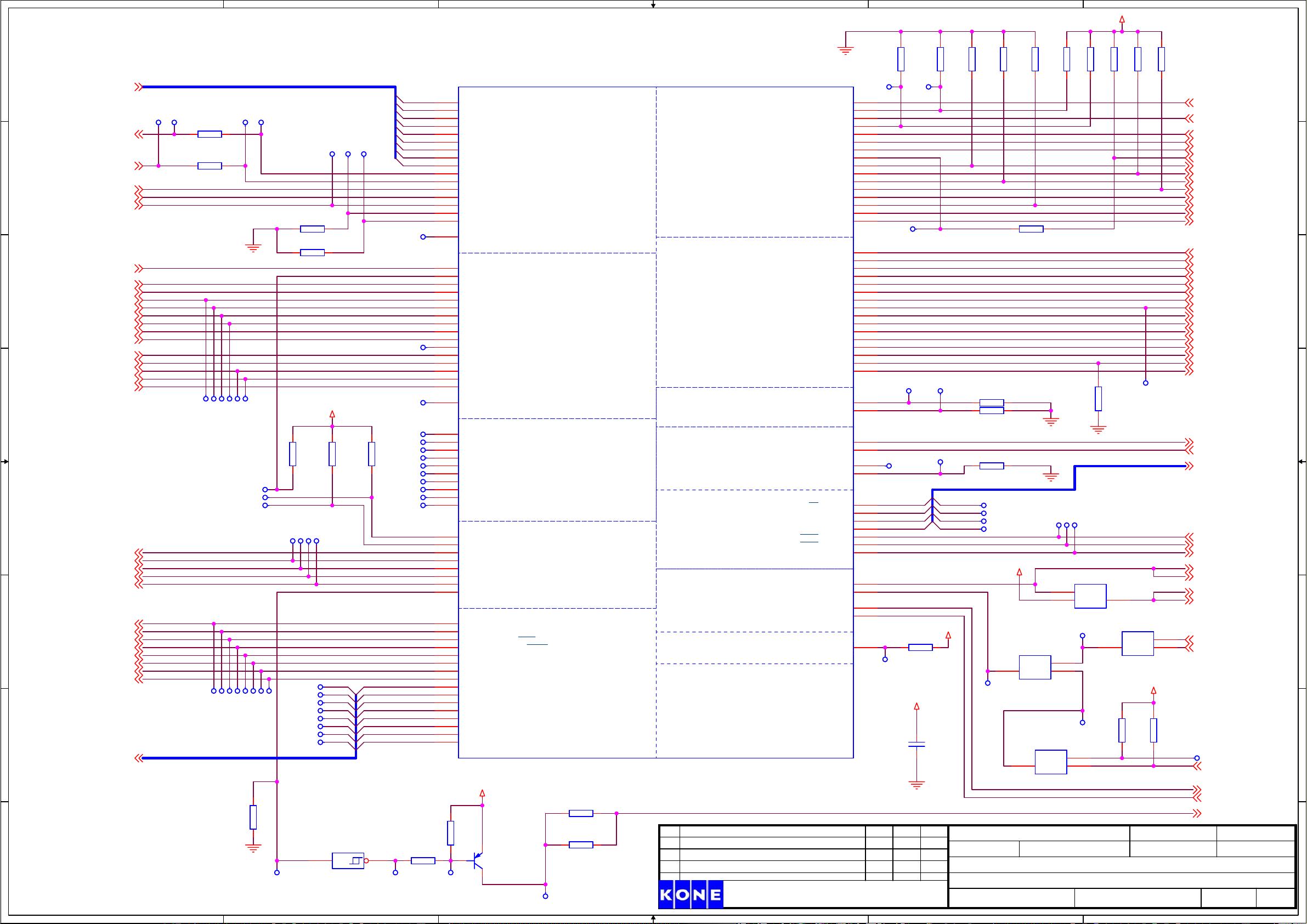
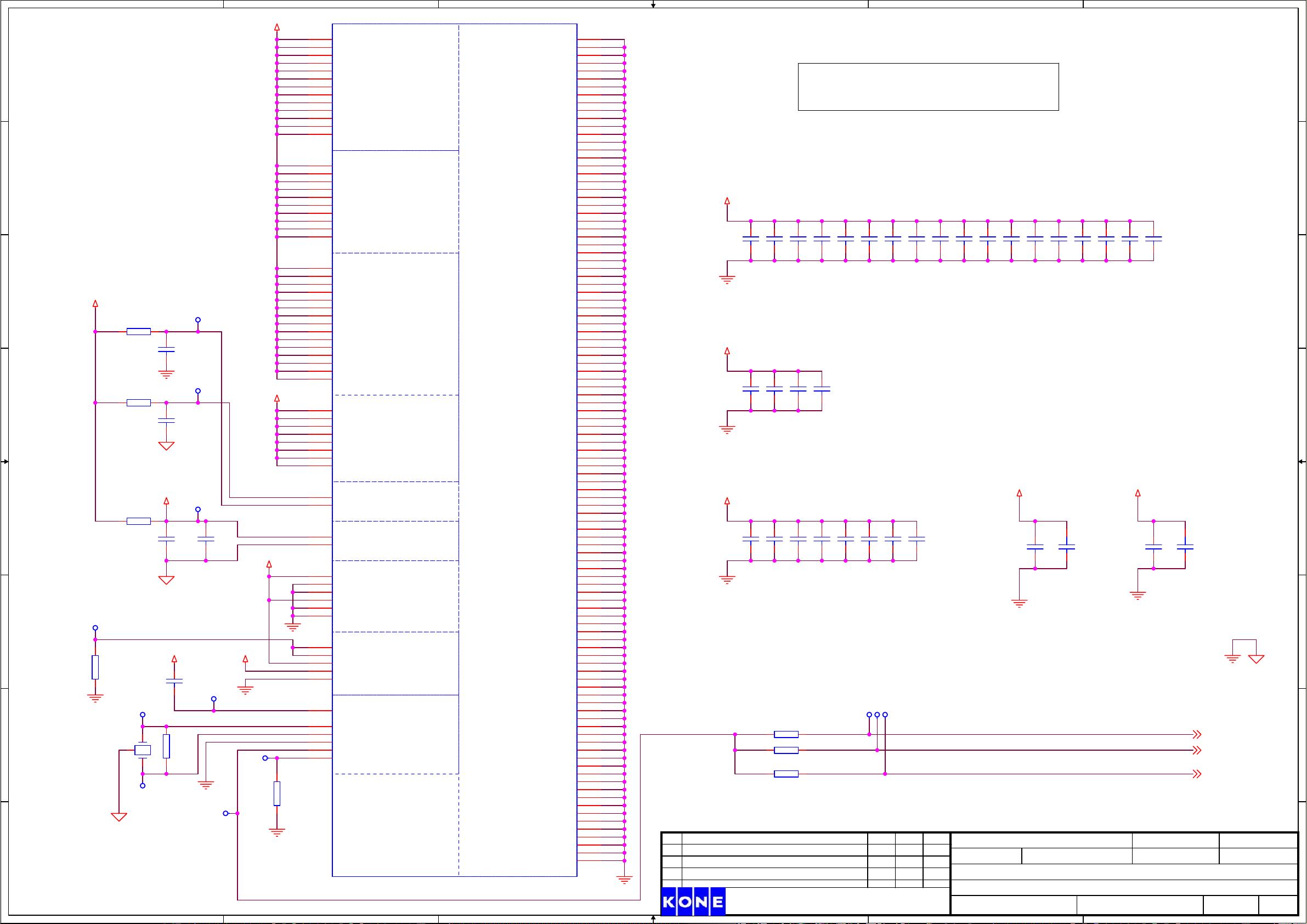
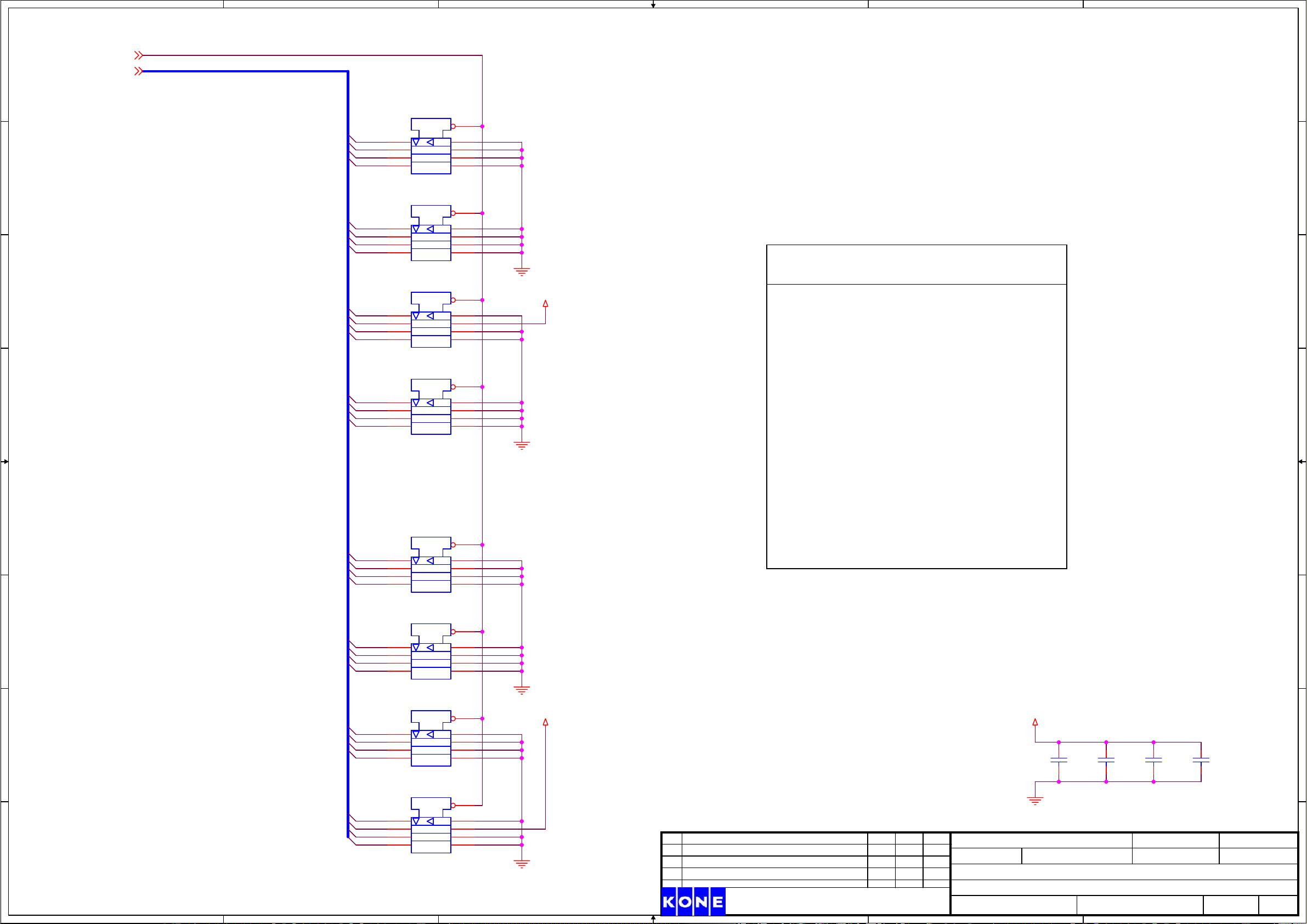
Processor bus
kttjah
F
12.5.2003
F
kttjah
13.9.2006
No Changes to this sheet
Issue
of
Change description Date Des. by Appr. by
Designed by
Dept Date
Checked by
Approved by
Language
Product code
PageIssueDrawing no.Sales ref no.
Copyright (C) 2001 KONE Corporation. All rights reserved under International Copyright Conventions.
No part of the contents of this document may be copied, reproduced or transmitted in any form or by any means,
or translated into another language or format, in whole or part, without written consent of KONE Corporation.
121
En
LCE
<Appr by>
<Chkd by>
Antti Toivonen
Konette
773391
LCECPU561
D
E
kttova 030805
K1706-1 replaced with CANPLD, see parts list
No Changes to this sheet 3.2.2006
Processor bus
kttjah
F
12.5.2003
F
kttjah
13.9.2006
No Changes to this sheet
CLOCK SOURCE
CONFIGURATION
BDM DEBUG-
CONNECTOR
RSTIN comparator level 1.22 V
2.6V voltage reset level 2.44 V
ENABLE BDM
JUMPER
CU8
NOTE: +3.3V
NOTE: +3.3V
Optional
resistor for
MAX6355
E46E46
E21E21
E104E104
R10
4.75K
R10
4.75K
R2
10.00K
R2
10.00K
E36E36
E55E55
E27E27
R1
47.5K
R1
47.5K
R16
4.75K
R16
4.75K
31
42
S12S12
E19E19
E77E77
E926E926
R9
5.62K
R9
5.62K
E57E57
R470
5.62K
R470
5.62K
E18E18
E83E83
E44E44
E10E10
E91E91
E25E25
E73E73
E47E47
E34E34
R471
4.75K
R471
4.75K
1
2
4
6
8 12
14
16
18
EN
U8A
74VHC244
EN
U8A
74VHC244
R15
4.75K
R15
4.75K
E37E37
E16E16
E8E8
E50E50
E105E105
E64E64
E29E29
E86E86
R425
274R
R425
274R
E68E68
R8
5.62K
R8
5.62K
R3
10.00K
R3
10.00K
E85E85
E42E42
E967E967
E32E32
E45E45
E59E59
E14E14
E90E90
E69E69
E100E100
E35E35
E66E66
19
11
13
15
17 3
5
7
9
EN
U8B
74VHC244
EN
U8B
74VHC244
ADDR_SGPIOA8
AF9
ADDR_SGPIOA9
AF8
ADDR_SGPIOA10
AC6
ADDR_SGPIOA11
Y4
ADDR_SGPIOA12
Y3
ADDR_SGPIOA13
AD7
ADDR_SGPIOA14
AE7
ADDR_SGPIOA15
AF7
ADDR_SGPIOA16
AD8
ADDR_SGPIOA17
AE8
ADDR_SGPIOA18
AC7
ADDR_SGPIOA19
AD9
ADDR_SGPIOA20
AC8
ADDR_SGPIOA21
AD10
ADDR_SGPIOA22
AF10
ADDR_SGPIOA23
AC9
ADDR_SGPIOA24
AD11
ADDR_SGPIOA25
AD12
ADDR_SGPIOA26
AC11
ADDR_SGPIOA27
AF11
ADDR_SGPIOA28
AE11
ADDR_SGPIOA29
AE12
ADDR_SGPIOA30
AE10
ADDR_SGPIOA31
AE9
DATA_SGPIOD0
AD13
DATA_SGPIOD1
AC12
DATA_SGPIOD2
AF14
DATA_SGPIOD3
AF13
DATA_SGPIOD4
AF15
DATA_SGPIOD5
AC13
DATA_SGPIOD6
AF16
DATA_SGPIOD7
AC14
DATA_SGPIOD8
AF17
DATA_SGPIOD9
AC16
DATA_SGPIOD10
AF18
DATA_SGPIOD11
AC17
DATA_SGPIOD12
AC18
DATA_SGPIOD13
AD18
DATA_SGPIOD14
AC20
DATA_SGPIOD15
AD19
DATA_SGPIOD16
AD20
DATA_SGPIOD17
AE20
DATA_SGPIOD18
AF20
DATA_SGPIOD19
AE19
DATA_SGPIOD20
AF19
DATA_SGPIOD21
AE18
DATA_SGPIOD22
AD17
DATA_SGPIOD23
AE17
DATA_SGPIOD24
AD16
DATA_SGPIOD25
AE16
DATA_SGPIOD26
AD15
DATA_SGPIOD27
AE15
DATA_SGPIOD28
AD14
DATA_SGPIOD29
AE14
DATA_SGPIOD30
AE13
DATA_SGPIOD31
AF12
IRQ0_SGPIOC0_MDO4
P3
IRQ1_RSV_SGPIOC1
P4
IRQ2_CR_SGPIOC2_MTS
P2
IRQ3_KR_RETRY_SGPIOC3
N1
IRQ4_AT2_SGPIOC4
P1
IRQ5_SGPIOC5_MODCK1
AD21
IRQ6_MODCK2
AE21
IRQ7_MODCK3
Y24
PORESET_TRST
W25
HRESET
W23
SRESET
W24
RSTCONF_TEXP
Y25
CS0
U1
CS1
U2
CS2
U3
CS3
U4
SGPIOC7_IRQOUT_LWP0
R1
WE0_BE0_AT0
T1
WE1_BE1_AT1
T2
WE2_BE2_AT2
T3
WE3_BE3_AT3
T4
TSIZ0
V4
TSIZ1
W1
OE
V2
RD/WR
V1
BURST
Y1
BDIP
W4
TS
W2
TA
W3
TEA
V3
BI_STS
Y2
BG_VF0_LWP1
R3
BR_VF1_IWP2
R4
BB_VF2_IWP3
R2
IWP0_VFLS0
N2
IWP1_VFLS1
N3
TMS_EVTI
M2
TDI_DSDI_MDI0
M1
TCK_DSCK_MCKI
L2
TDO_DSDO_MDO0
M4
JCOMP_RSTI
L1
SGPIOC6_FRZ_PTR
N4
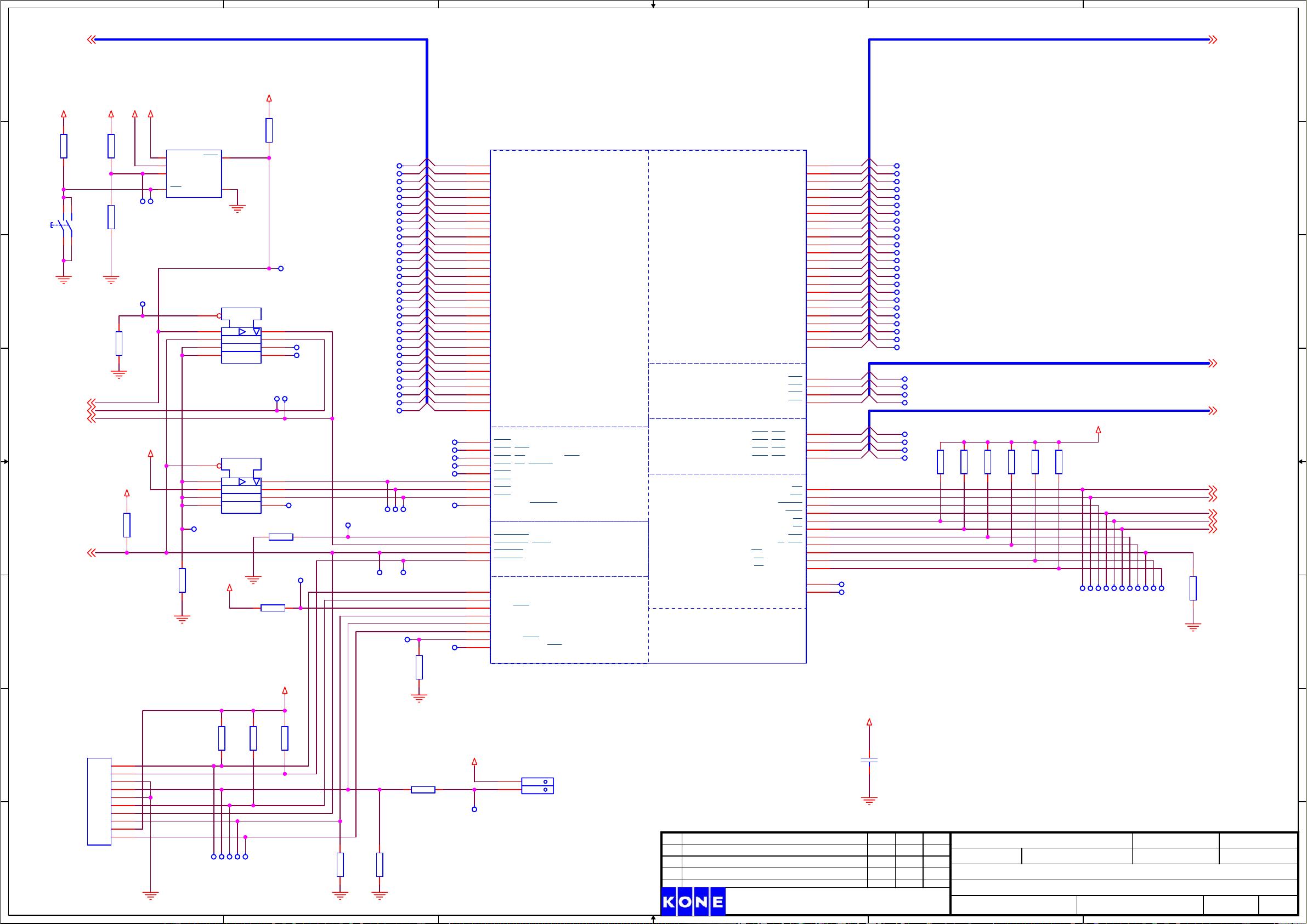
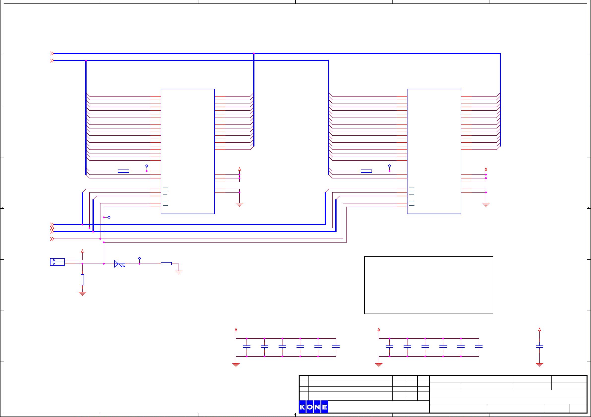
MPC 561/563 part 1/3:
Bus interface
Data bus
GPIO
Address bus
GPIO
Chip selects
Write/byte enables
Bus control signals
Reset signals
Interrupts
CLK config
GPIO
BDM/JTAG
Debug interface
U7A
MPC561
MPC 561/563 part 1/3:
Bus interface
Data bus
GPIO
Address bus
GPIO
Chip selects
Write/byte enables
Bus control signals
Reset signals
Interrupts
CLK config
GPIO
BDM/JTAG
Debug interface
U7A
MPC561
E30E30
E15E15
E4E4
E40E40
E78E78
R6
5.62K
R6
5.62K
E70E70
E49E49
R13
4.75K
R13
4.75K
E51E51
E54E54
E13E13
E61E61
E80E80
E79E79
E11E11
E95E95
E48E48
E28E28
E3E3
E89E89
E60E60
E38E38
E67E67
E102E102
E43E43
E84E84
E96E96
R5
5.62K
R5
5.62K
E9E9
E12E12
E72E72
E101E101
E76E76
E6E6
E968E968
E65E65
1
2
3
4
5
6
7
8
9
10
XBDM1
2x5pin-2,54mm-180°
XBDM1
2x5pin-2,54mm-180°
E26E26
E52E52
E82E82
E39E39
E94E94
E1015E1015
E62E62
E99E99
E98E98
E103E103
E7E7
C253
47nF
C253
47nF
E88E88
E71E71
E74E74
R12
4.75K
R12
4.75K
E63E63
E31E31
E24E24
E58E58
E33E33
E93E93
E17E17
R7
5.62K
R7
5.62K
1
2
BR1
PINH
1
2
BR1
PINH
E81E81
E5E5
E1E1
R14
4.75K
R14
4.75K
E22E22
E87E87
R4
5.62K
R4
5.62K
R20
4.75K
R20
4.75K
R21
20.0K
R21
20.0K
E75E75
MR
3
VCC3
4
RST
1
GND
2
VCC5
6
RSTIN
5
MAX6355
U6
MAX6355
U6
E53E53
R11 4.75KR11 4.75K
E56E56
E23E23
E41E41
R19
2.21K
R19
2.21K
R424
1.00K
R424
1.00K
E92E92
E2E2
E20E20
剩余20页未读,继续阅读
资源评论


无际-学无边际
- 粉丝: 10
- 资源: 18


