LIANG et al.: 9.1ENOB 200MS/s ASYNCHRONOUS SAR ADC WITH HYBRID SINGLE-ENDED/DIFFERENTIAL DAC 7131
performance. Adopting hybrid architecture is also an effective
solution to improve the sampling rate [9]. Unfortunately,
although the pipeline-SAR ADC is more energy-efficient
than the pipeline ADC on some level, it still faces similar
difficulties to those of the pipeline ADC. The flash-SAR ADC
can succeed in improving the sampling rate and be compatible
with the scaling process at the sacrifice of power efficiency.
The non-binary weighted SAR ADC is able to overcome the
DAC’s incomplete settling issues, but the layout of the capac-
itive DAC is hard to design to meet the matching requirement,
which can degrade the ADC linearity and introduce high-order
harmonics. In addition, the digital error correction (DEC)
logic for the non-binary weighted SAR ADC is also too
complicated [10]. Compared to the non-binary weighted SAR
ADC, the binary weighted SAR ADC with redundant bits can
be easier to design. But the binary weighted SAR ADC fails
to compensate the incomplete settling in every comparison
cycle [11]. Liu et al. [12] proposed a Binary-Scaled Recombi-
nation Weighting Method. With the method proposed in [12],
no additional compensation capacitor is truly needed. But the
DEC logic still brings about power consumption that cannot
be overlooked, especially in the high-speed case. Besides this,
it is noteworthy that realizations of the methods proposed
in [13] and [14], without exception, call for additional
comparison cycles. As a result, given the ADC resolution and
throughput, the comparator design is faced with an increasing
challenge.
In this paper, a single-channel 9.1ENOB 200MS/s asyn-
chronous SAR ADC at 1.2V supply is designed in 55nm
CMOS technique. To reduce the LDO static power and circuit
complexity, only one reference Vref, which is generated by the
on-chip LDO and supplies the ADC, is required. Besides this,
the ADC performance cannot be affected by the accuracy of
Vref since no other reference but Vref is involved in the ADC
conversion phase [15]. It is known that the ADC linearity
can be degraded if the comparator common mode voltage
V
COM
changes in the course of conversion [7]. On account
of this, a symmetrical switching method in the proposed
ADC is employed to realize a constant V
COM
. Beyond this,
a comparison-cycle self-adjusting technique, which aims at
adjusting the settling time allocated for different weighed
capacitors in the DACs automatically, is utilized to guarantee
the settling accuracy for high-weighed capacitors.
The paper is organized as follows. Section II describes the
overall SAR ADC architecture. Section III introduces
the circuit implementation of each building block.
Section IV provides a die photograph and layout of the
proposed ADC. Measured results for both single-ended and
differential operation mode are also presented in this section.
Finally, the features of the proposed ADC are summarized in
Section V.
II. SAR ADC A
RCHITECTURE
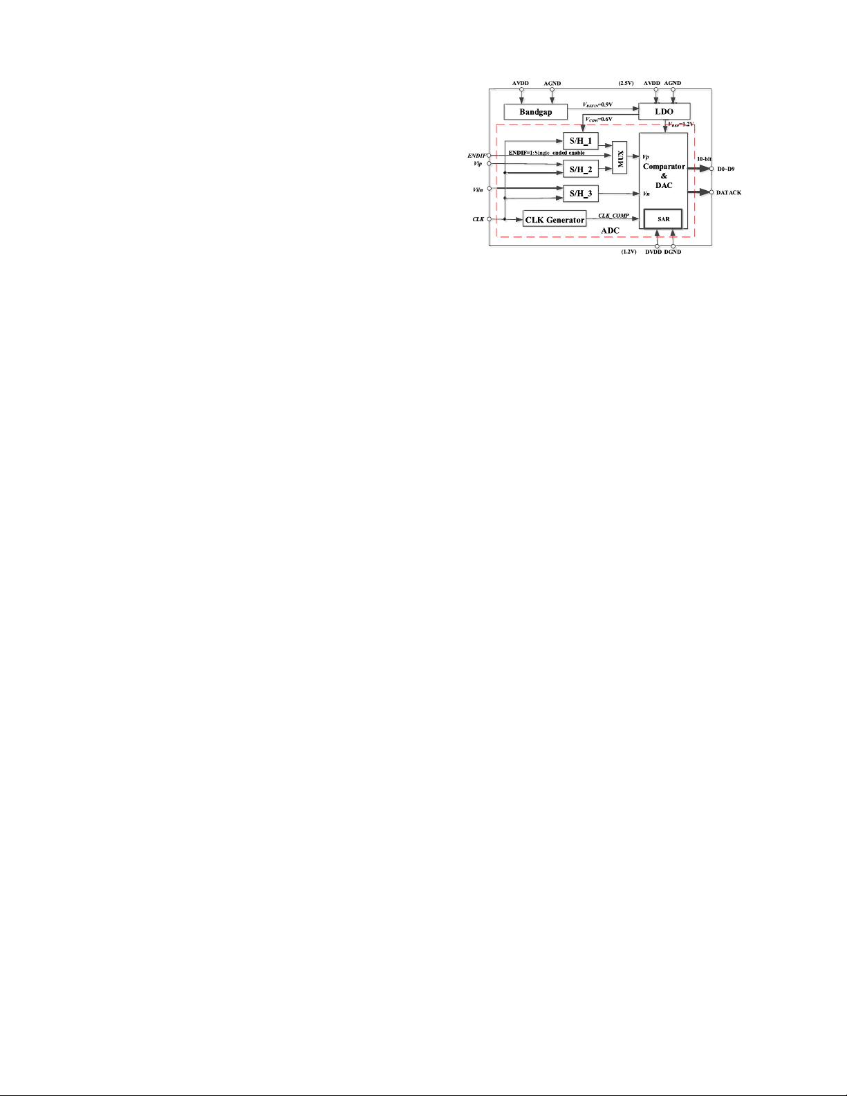
Fig. 2 illustrates the architecture of the proposed SAR ADC.
It is composed of a bandgap block, an open-loop fast-response
LDO and a 10-bit capacitive SAR ADC.
The bandgap generates a 0.9-V zero-temperature-coefficient
reference, which is the input of the LDO. V
REF
provided by
Fig. 2. Architecture of the proposed SAR ADC.
the on-chip LDO serves as the analog supply of the capacitive
DAC, the comparator and the bootstrapped switches, while the
off-chip 1.2V DVDD serves as the supply of digital cells of the
SAR ADC, which always operate at a high frequency. In this
way, V
REF
succeeds in avoiding being contaminated by the
switching noise from DVDD. To ensure the comparator makes
correct decisions in every comparison cycle, the LDO output
should settle accurately every time before the comparator oper-
ates. The ADC core consists of two binary-weighted capacitive
DACs, a low-power high-speed dynamic latch comparator,
an asynchronous SAR digital logic, a comparison-cycle self-
adjusting clock generator, a 2-path multiplexer and three
bootstrapped switches executing the sample-and-hold function.
A binary-weighted structure for capacitive DACs in the SAR
ADC is always a preferred choice, since it features better
matching ability. The dynamic latch comparator determines
the values of the output bits according to its inputs Vp and Vn,
which are also the voltages on the bottom plates in the
differential capacitor DACs. Next, the outputs bits, from the
MSB bit to the LSB bit, are successively fed to the control
logic, which controls the switching action of the DACs. Then
the differential DACs convert the output of the SAR logic to
analog values by switching the capacitors to different voltage
references. For an N-bit SAR ADC, after N comparison
cycles, one conversion is complete. When the enable signal
ENDIF is high, the single-ended operation mode is activated.
Bootstrapped switches S/H_1 and S/H_3 are switched on,
while S/H_2 is off. At this time, the positive input of the
capacitive DAC is the 0.6-V common-mode voltage, and the
negative input is the single-ended input signal. On the contrary,
when the enable signal ENDIF is low, the differential operation
mode is activated. At that time, S/H_2 and S/H_3 are switched
on to sample the differential input signals,while S/H_1 is off.
III. C
IRCUIT IMPLEMENTATION
A. Capacitive DAC
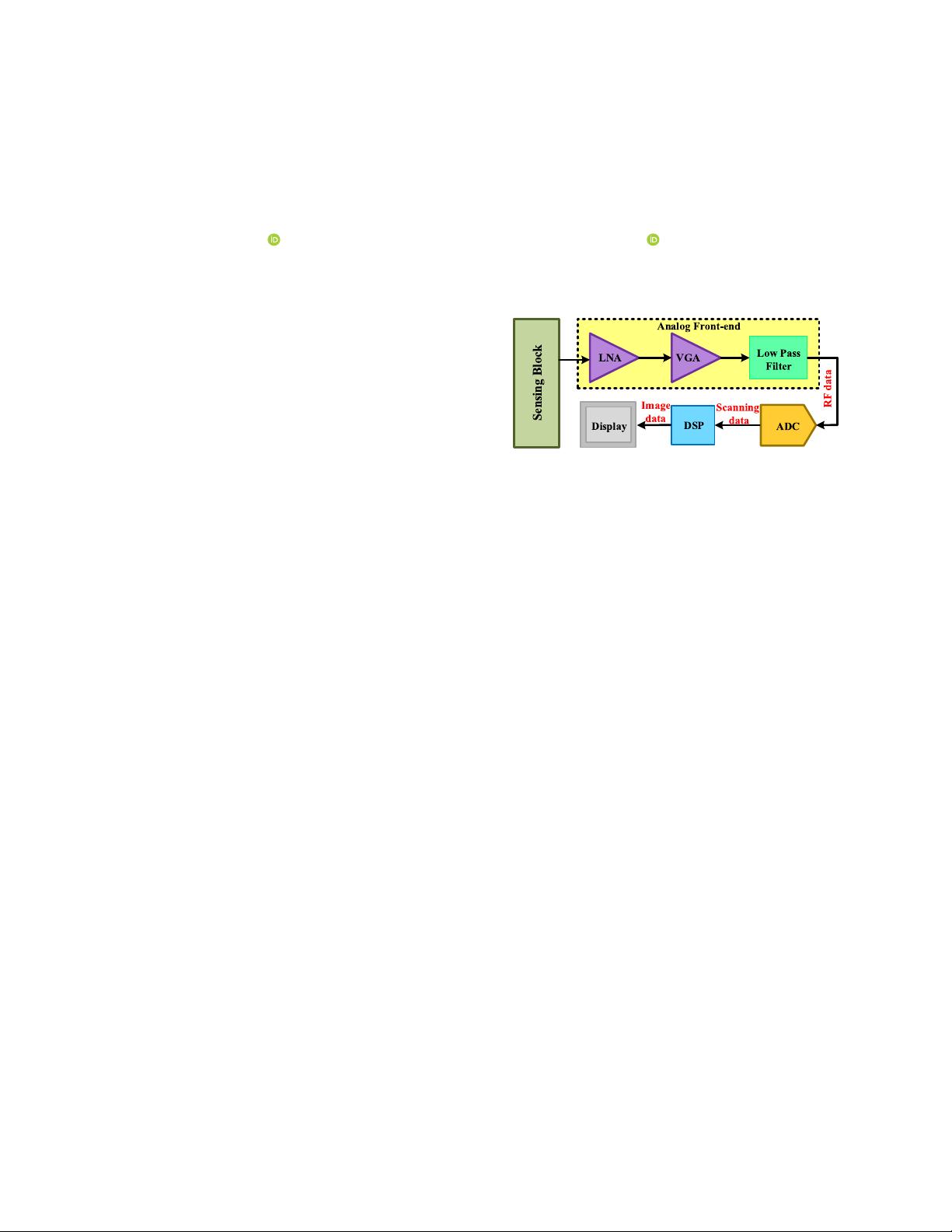
The image sensor signals are generally single-ended sig-
nals [16]. Both single-ended and differential architectures
can be chosen for SAR ADCs to deal with image sensor
signals [17], [18]. Compared with the differential counterpart,
the single-ended architecture requires a smaller chip area
and consumes lower power. Nevertheless, performance of the
single-ended ADCs always suffers from the contamination of


 我的内容管理
展开
 我的资源
快来上传第一个资源
 我的收益 登录查看自己的收益
 我的积分
登录查看自己的积分
 我的C币
登录后查看C币余额
 我的收藏
我的收藏  我的下载
我的下载  下载帮助
下载帮助 
 前往需求广场,查看用户热搜

 信息提交成功