
© Semiconductor Components Industries, LLC, 2011
March, 2011 − Rev. 3
1 Publication Order Number:
CM1442/D
CM1442
LCD and Camera EMI Filter
Array with ESD Protection
Product Description
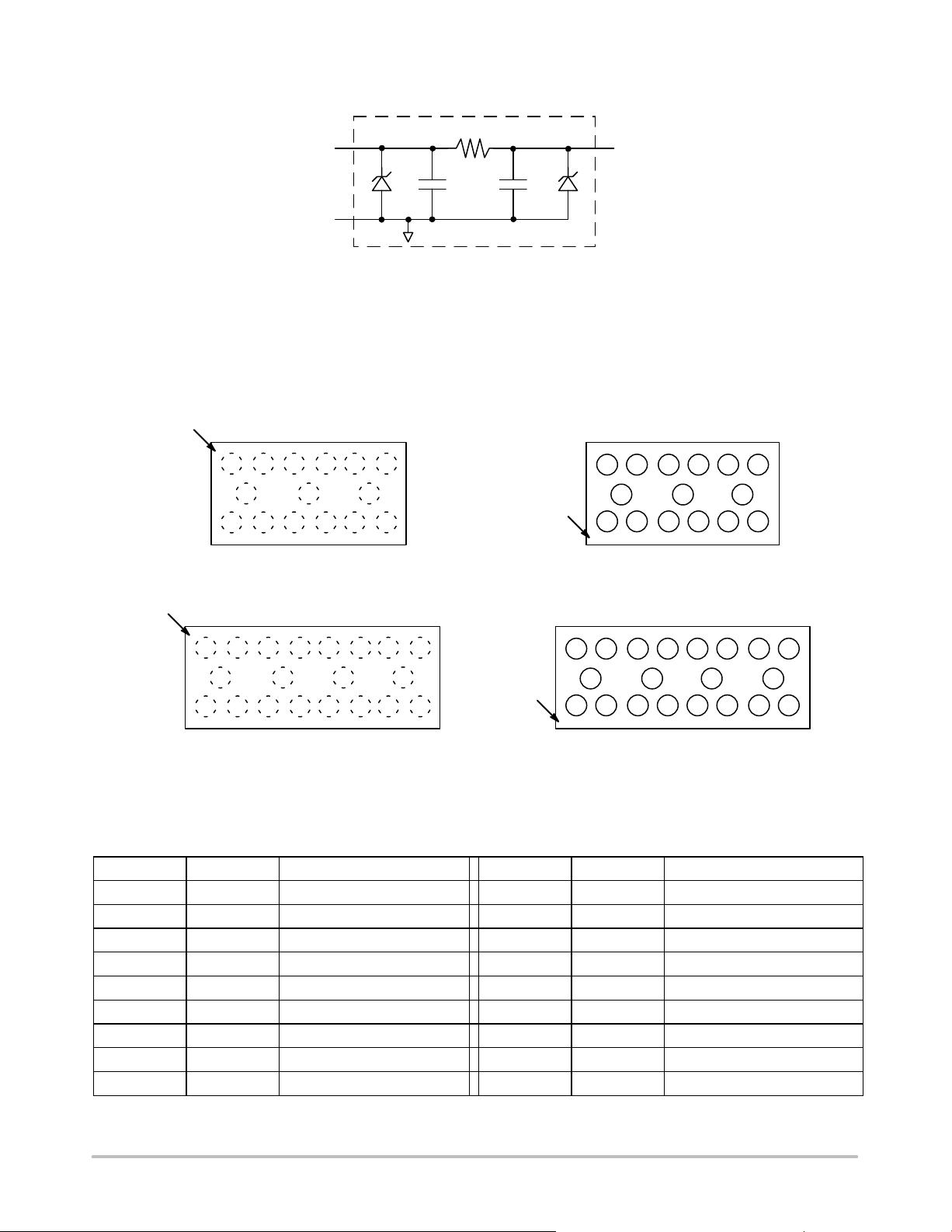
The CM1442 is a family of pi−style EMI filter arrays with ESD
protection, which integrates six and eight filters (C−R−C) in Chip
Scale Package form factor with 0.40 mm pitch. The CM1442 has
component values of 15 pF − 100 W − 15 pF per channel. The CM1442
has a cut−off frequency of 120 MHz and can be used in applications
where the data rates are as high as 48 Mbps. The parts include
avalanche−type ESD diodes on every pin, which provide a very high
level of protection for sensitive electronic components that may be
subjected to electrostatic discharge (ESD). The ESD protection diodes
safely dissipate ESD strikes of ±15 kV, well beyond the maximum
requirement of the IEC61000−4−2 international standard. Using the
MIL−STD−883 (Method 3015) specification for Human Body Model
(HBM) ESD, the pins are protected for contact discharges at greater
than ±30 kV.
This device is particularly well suited for portable electronics (e.g.
wireless handsets, PDAs, notebook computers) because of its small
package format and easy−to−use pin assignments. In particular, the
CM1442 is ideal for EMI filtering and protecting data and control lines
for the I/O data ports, LCD display and camera interface in mobile
handsets.
The CM1442 incorporates OptiGuardt which results in improved
reliability at assembly. The CM1442 is available in a space−saving,
low−profile Chip Scale Package with RoHS compliant lead−free
finishing. It is manufactured with a 0.40 mm pitch and 0.25 mm CSP
solder ball to provide up to 28% board space saving versus competing
CSP devices with 0.50 mm pitch and 0.30 mm CSP solder ball.
Features
• Six and Eight Channels of EMI Filtering with Integrated ESD
Protection
• 0.4 mm Pitch, 15−Bump, 2.360 mm x 1.053 mm Footprint Chip
Scale Package (CM1442−06)
• 0.4 mm Pitch, 20−Bump, 3.160 mm x 1.053 mm Footprint Chip
Scale Package (CM1442−08)
• Pi−Style EMI Filters in a Capacitor−Resistor−Capacitor
(C−R−C) Network
• ±15 kV ESD Protection on Each Channel
(IEC 61000−4−2 Level 4, Contact Discharge)
• ±30 kV ESD Protection on Each Channel (HBM)
• Greater than 30 dB Attenuation (Typical) at 1 GHz
• Chip Scale Package Features Extremely Low Lead
Inductance for Optimum Filter and ESD Performance
• OptiGuardtCoated for Improved Reliability at
Assembly
• These Devices are Pb−Free and are RoHS Compliant
Applications
• LCD and Camera Data Lines in Mobile Handsets
• I/O Port Protection for Mobile Handsets, Notebook
Computers, PDAs, etc.
• Wireless Handsets
• EMI Filtering for Data Ports in Cell Phones, PDAs or
Notebook Computers
• Handheld PCs/PDAs
• LCD and Camera Modules
MARKING DIAGRAM
Device Package Shipping
†
ORDERING INFORMATION
http://onsemi.com
CM1442−06CP CSP−15
(Pb−Free)
3500/Tape & Reel
N426 = CM1442−06CP
N428 = CM1442−08CP
N426
CM1442−08CP CSP−20
(Pb−Free)
3500/Tape & Reel
CM1442−06
15−Bump CSP Package
N428
CM1442−08
20−Bump CSP Package
WLCSP20
CP SUFFIX
CASE 567BU
†For information on tape and reel specifications,
including part orientation and tape sizes, please
refer to our Tape and Reel Packaging Specification
Brochure, BRD8011/D.
WLCSP15
CP SUFFIX
CASE 567BP
剩余10页未读,继续阅读
资源评论


