

Layer-number determination of two-dimensional
materials by optical characterization
You Zheng (郑 优), Changyong Lan (兰长勇), Zhifei Zhou (周智飞), Xiaoying Hu (胡晓影),
Tianying He (何天应), and Chun Li (李 春)*
State Key Laboratory of Electronic Thin Films and Integrated Devices, and School of Optoelectronic Information,
University of Electronic Science and Technology of China, Chengdu 610054, China
*Corresponding author: lichun@uestc.edu.cn
Received October 29, 2017; accepted December 12, 2017; posted online January 29, 2018
Initiated by graphene, two-dimensional (2D) layered materials have attracted much attention owing to their
novel layer-number-dependent physical and chemical properties. To fully utilize those properties, a fast and
accurate determination of their layer number is the priority. Compared with conventional structural charac-
terization tools, including atomic force microscopy, scanning electron microscopy, and transmission electron
microscopy, the optical characterization methods such as optical contrast, Raman spectroscopy, photolumines-
cence, multiphoton imaging, and hyperspectral imaging have the distinctive advantages of a high-throughput
and nondestructive examination. Here, taking the most studied 2D materials like graphene, MoS
2
, and black
phosphorus as examples, we summarize the principles and applications of those optical characterization
methods. The comparison of those methods may help us to select proper ones in a cost-effective way.
OCIS codes: 120.6200, 160.4760, 180.5655, 310.6860.
doi: 10.3788/COL201816.020006.
Micromechanical exfoliated graphene opened the research
field of two-dimensional (2D) materials. Since then, more
and more 2D layered materials, including molybdenum
sulfide (MoS
2
), hexagonal boron nitride (h-BN), black
phosphorus (BP), and so on, have been reported and have
attracted great interest. Compared with conventional
electronic and optical materials, 2D materials show many
unique properties such as record-high charge carrier
mobility, strong light–matter interaction, and superior
mechanical properties
[1–3]
, which implies promising appli-
cations for novel devices
[4]
. However, many of those fasci-
nating properties are strongly dependent on their layer
numbers (LNs). For example, monolayer graphene has
a zero ban dgap, while bilayer graphene on SiC substrate
has a finite bandgap of ∼0.26 eV
[5]
. Monolayer MoS
2
is a
direct bandgap semiconductor, but bilayer MoS
2
is an
indirect one. While the bandgap of BP decreases as the
number of layers increases from monolayer (1.5–2.0 eV)
to bulk (0.2 eV)
[6]
. In addition, at present, it is still a great
challenge to precisely contro l the LN of 2D materials in
large scale, although there are many methods for prepar-
ing 2D materials including micromechanical exfoliation
[7]
,
epitaxial growth
[8]
, chemical vapor deposition (CVD)
[9]
,
and liquid phase exfoliation
[10]
. Therefore, it is critical to
find an efficient and reliable way to identify their LNs,
which is important for both fundamental research and in-
dustrial application.
Among the numerous thickness characterization meth-
ods, atomic force microscopy (AFM), scanning electron
microscopy (SEM), and transmission electron microscopy
(TEM) are the most intuitive approaches. Nevertheless,
these structural characterization methods are usually
low in throughput, prone to sample damage, and strict
with substrate choosing. For example, during the measur-
ing process of AFM in contact mode, the cantilever tip
always needs contacting with the sample, which may
cause irreversible physical damage to the samples. In
the SEM observation, conductive substrates are required
to eliminate the charge accumulation. The low-voltage
mode is much sensitive to small surface features but de-
creases the signal-to-noise ratio. The TEM characteriza-
tion requires sophistica ted skills and experiences with
sample preparation. For optical characterization, due to
the strong LN-dependent light–matter interactions of
2D materials, the variation of optical signals collecting
from the scattering, absorption, or light emission can be
correlated to the LNs. Therefore, by detecting these opti-
cal signals and interpreting their peak position, intensity,
and line shape associated with LNs, their exact LNs can be
accurately determined. Such an optical characterization is
nondestructive, with high throughput, and reliable. Here,
we review the principles and recent development of the
commonly adopted optical characterization methods,
and compare their advantages and limitations.
This review is organized as follows. After the introduc-
tion, we first focus on the most frequently used method,
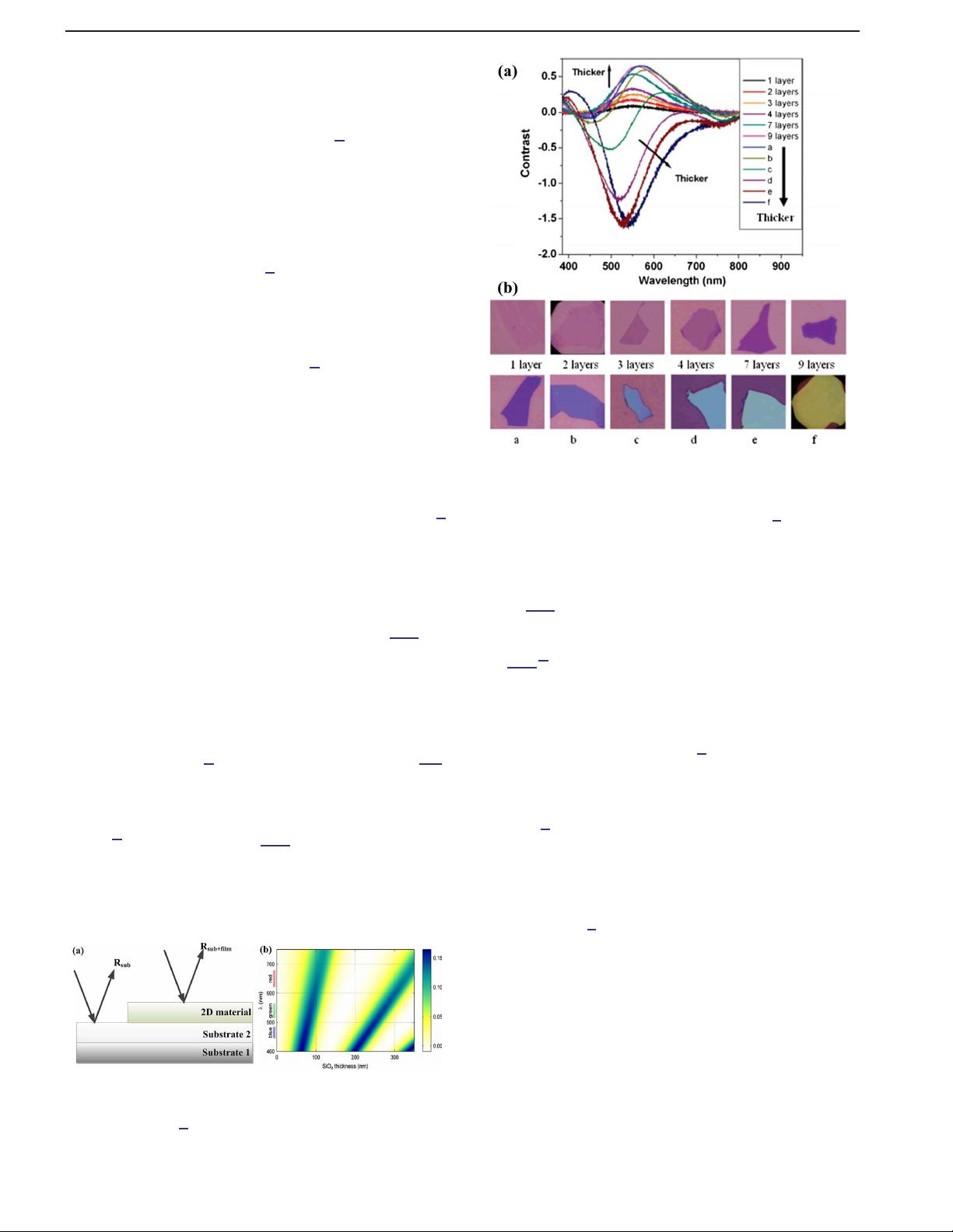
the reflective optical contrast, to identify the LNs of 2D
materials laying on nontransparent substrates. Particu-
larly, we summarize the reported strategies on improving
the visibility of 2D materials by engineering the reflection
contrast of the substrates. Then, Raman and photolumi-
nescence (PL) characterizations of typical 2D materials
(graphene, MoS
2
, and BP) are briefly reviewed. The mul-
tiphoton spectrum relying on nonlinear absorption is
one of the focuses in another section. Other methods
mainly regarding the identification of 2D materials on
COL 16(2), 020006(2018) CHINESE OPTICS LETTERS February 10, 2018
1671-7694/2018/020006(7) 020006-1 © 2018 Chinese Optics Letters
剩余6页未读,继续阅读
资源评论


weixin_38523728
- 粉丝: 3
- 资源: 973


最新资源
- 2015-2024年上市公司商道融绿esg评级数据(年度)
- DeepSeek:通用人工智能从入门到精通的技术解析与应用指南
- 离散扩展龙伯格观测器:扰动补偿功能下的鲁棒性能优化及动态响应增强策略,离散扩展龙伯格观测器:具有扰动补偿功能的高鲁棒性预测控制系统,一种具有扰动补偿功能的离散扩展龙伯格观测器,有较好的参数摄动扰动抑制
- 无刷直流电机BLDC三闭环控制系统的Matlab Simulink仿真模型搭建:原理、波形记录与参数详解,无刷直流电机BLDC三闭环控制系统的Matlab Simulink仿真模型搭建:原理、波形记录
- 基于Python的Django-vue基于spark的短视频推荐系统的设计与实现源码-说明文档-演示视频.zip
- DeepSeek写的重力球迷宫手机小游戏
- 单相变压器绕组与铁芯振动形变仿真模型:洛伦兹力与磁致伸缩效应下的动态响应分析,COMSOL单相变压器绕组与铁芯振动形变仿真模型:基于洛伦兹力与磁致伸缩效应的时域分析,comsol的单相变压器绕组及铁芯
- 新兴经济体二氧化碳排放报告2024.pdf
- 激光熔覆技术:COMSOL模拟建模与视频教程服务,助力激光研究人员与工程师的专业提升,激光熔覆技术:COMSOL软件下的建模与视频教程应用指南,COMSOL 激光 激光熔覆 名称:激光熔覆 适用人群:
- 2000-2023年上市公司价值链升级数据(含原始数据+计算代码+结果)
- COMSOL仿真下的钢架无损超声检测:焊接区域及周边缺陷识别技术,角钢梁纵波转横波检测原理揭秘,Comsol仿真技术下的钢架无损超声检测:角钢梁缺陷的精准识别与定位,Comsol仿真钢架无损超声检测
- 基于FPGA的图像坏点像素修复算法实现及Matlab辅助验证:探索其原理、测试与使用视频教程 注:标题中的“可刀”一词在此上下文中并无实际意义,因此未被包含在标题中 标题长度符合要求,并尽量简洁明了
- 2008-2022年各省环境污染指数数据(原始数据+结果).xlsx
- zhaopin_mzhan.apk
- 权威科研机构发布钢轨表面缺陷检测数据集,含400张图像和8种类别缺陷,mAP达0.8,附赠lunwen,钢轨表面缺陷检测数据集:包含400张图片与八种缺陷类别,适用于目标检测算法训练与研究 ,钢轨表面
- C形永磁辅助同步磁阻电机Maxwell参数化模型:转子手绘设计及关键参数优化分析,基于Maxwell参数化模型的C形永磁辅助同步磁阻电机研究:转子手绘非UDP模块的参数化设计及优化分析,C形永磁辅助同
资源上传下载、课程学习等过程中有任何疑问或建议,欢迎提出宝贵意见哦~我们会及时处理!
点击此处反馈


