没有合适的资源?快使用搜索试试~ 我知道了~
pipeline ADC的设计指南
需积分: 5 3 下载量 152 浏览量
2023-12-14
14:18:16
上传
评论 1
收藏 5.15MB PDF 举报
温馨提示
试读
124页
pipeline ADC的设计指南
资源推荐
资源详情
资源评论
Department of Electrical and Computer Engineering
Slides by Bibhudatta Sahoo
-1-
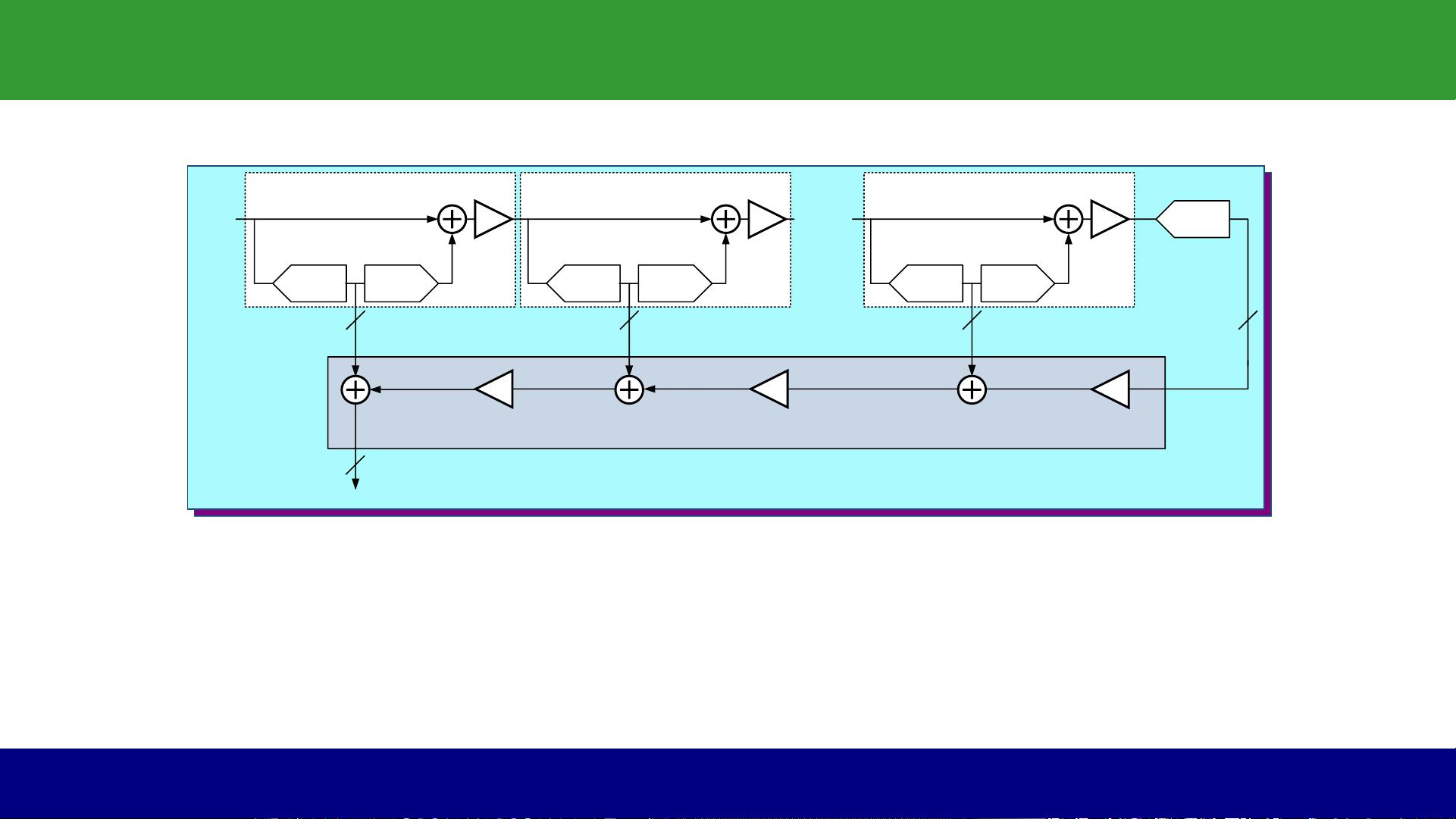
Pipelined ADC Design
- A Tutorial -
Based on Slides from Dr. Bibhudatta Sahoo
University of Illinois at Urbana-Champaign
Slides by Bibhudatta Sahoo
-2-
2
Outline
Review of Pipelined ADCs
Impact of Scaling on Data Converter Design
Why Calibration?
Basics of Digital Calibration Techniques
Survey of Digital Calibration Techniques
Conclusion
Slides by Bibhudatta Sahoo
-3-
Introduction
Data Converter Design is challenging in Nanoelectronics Era:
Low intrinsic device gain
High nonlinearity
Reduced headroom (reduced dynamic range)
Large variability and mismatches
Survival in digital-driven system-on-chip (SOC) environment
Trends in data converter design
Digitally Assisted Analog Design
Fuelled by aggressive device scaling
3
Slides by Bibhudatta Sahoo
-4-
Pipeline ADC
- Review -
4
Slides by Bibhudatta Sahoo
-5-
5
Generic Pipelined ADC
Each stage resolves a small number of bits (i.e. N
1
, N
2
, …, N
M
bits).
The overall resolution of the ADC is P = (N
1
+N
2
+…+N
M
+N
M+1
).
Output of stage-i (called “residue” r
i
) is digitized to (P-
i
j=1
N
j
)-bits.
The low resolution ADC digitizing r
i
is called the backend of stage-i.
(N
1
+1)-bits
D
1
· ·
sub-DACsub-ADC
·
·
2
N
1
sub-DACsub-ADC
·
·
2
·
(N
2
+1)-bits
D
2
sub-DACsub-ADC
·
·
2
N
M
N
2
(N
M
+1)-bits
D
M
Flash
ADC
N
(M+1)
-bits
2
-N
1
2
-N
2
2
-N
M
V
IN
D
OUT
(N
1
+ N
2
+ …+ N
M
)-bits
Digital Combiner
Stage-1 Stage-2 Stage-M
+
-
+
-
+
-
剩余123页未读,继续阅读
资源评论
戒了你的狂
- 粉丝: 2813
- 资源: 5
上传资源 快速赚钱
- 我的内容管理 展开
- 我的资源 快来上传第一个资源
- 我的收益 登录查看自己的收益
- 我的积分 登录查看自己的积分
- 我的C币 登录后查看C币余额
- 我的收藏
- 我的下载
- 下载帮助
安全验证
文档复制为VIP权益,开通VIP直接复制
信息提交成功