没有合适的资源?快使用搜索试试~ 我知道了~
ads1110 datasheet
需积分: 46 6 下载量 45 浏览量
2022-04-14
21:09:32
上传
评论
收藏 1.26MB PDF 举报
温馨提示
试读
23页
ads1110数据表
资源详情
资源评论
资源推荐
SBAS276A − MARCH 2003 − REVISED NOVEMBER 2003
16-Bit ANALOG-TO-DIGITAL CONVERTER
with Onboard Reference
ADS1110
FEATURES
D COMPLETE DATA ACQUISITION SYSTEM IN
A TINY SOT23-6 PACKAGE
D ONBOARD REFERENCE:
Accuracy: 2.048V ±0.05%
Drift: 5ppm/°C
D ONBOARD PGA
D ONBOARD OSCILLATOR
D 16-BITS NO MISSING CODES
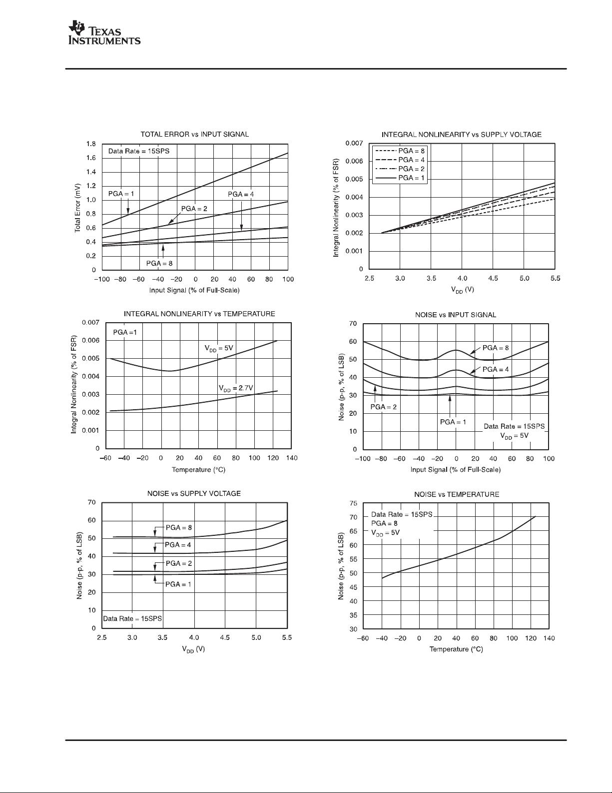
D INL: 0.01% of FSR max
D CONTINUOUS SELF-CALIBRATION
D SINGLE-CYCLE CONVERSION
D PROGRAMMABLE DATA RATE: 15SPS TO
240SPS
D I
2
CINTERFACE—EIGHT AVAILABLE
ADDRESSES
D POWER SUPPLY: 2.7V to 5.5V
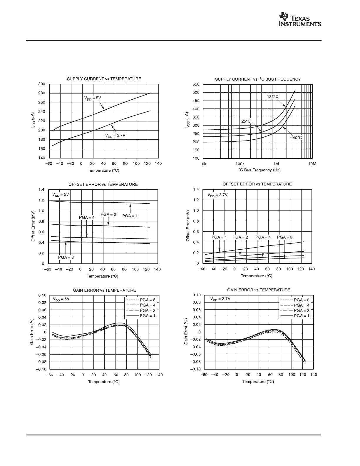
D LOW CURRENT CONSUMPTION: 240µA
APPLICATIONS
D PORTABLE INSTRUMENTATION
D INDUSTRIAL PROCESS CONTROL
D SMART TRANSMITTERS
D CONSUMER GOODS
D FACTORY AUTOMATION
D TEMPERATURE MEASUREMENT
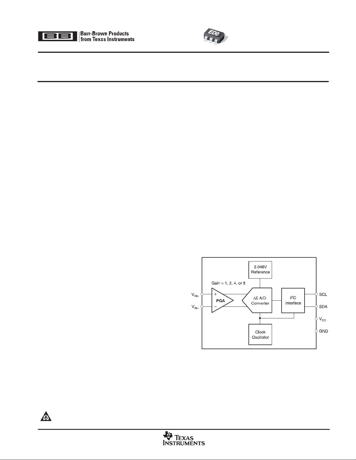
DESCRIPTION
The ADS1110 is a precision, continuously self−calibrating
Analog-to-Digital (A/D) converter with differential inputs and
up to 16 bits of resolution in a small SOT23-6 package. The
onboard 2.048V reference provides an input range of
±2.048V differentially. The ADS1110 uses an I
2
C-compatible
serial interface and operates from a single power supply
ranging from 2.7V to 5.5V.
The ADS1110 can perform conversions at rates of 15, 30, 60,
or 240 samples per second. The onboard programmable
gain amplifier (PGA), which offers gains of up to 8, allows
smaller signals to be measured with high resolution. In
single-conversion mode, the ADS1110 automatically powers
down after a conversion, greatly reducing current
consumption during idle periods.
The ADS1110 is designed for applications requiring
high-resolution measurement, where space and power
consumption are major considerations. Typical applications
include portable instrumentation, industrial process control,
and smart transmitters.
www.ti.com
Copyright 2003, Texas Instruments Incorporated
Please be aware that an important notice concerning availability, standard warranty, and use in critical applications of Texas Instruments
semiconductor products and disclaimers thereto appears at the end of this data sheet.
All trademarks are the property of their respective owners.
! !
ADS1110
SBAS276A − MARCH 2003 − REVISED NOVEMBER 2003
www.ti.com
2
ABSOLUTE MAXIMUM RATINGS
(1)
V
DD
to GND −0.3V to +6V
Input Current 100mA, Momentary
Input Current 10mA, Continuous
Voltage to GND, V
IN+
, V
IN−
−0.3V to V
DD
+ 0.3V
Voltage to GND, SDA, SCL −0.5V to 6V
Maximum Junction Temperature +150°C
Operating Temperature Range −40°C to +125°C
Storage Temperature Range −60°C to +150°C
Lead Temperature (soldering, 10s) +300°C
(1)
Stresses above those listed under “Absolute Maximum Ratings”
may cause permanent damage to the device. Exposure to
absolute maximum conditions for extended periods may affect
device reliability.
This integrated circuit can be damaged by ESD.
Texas Instruments recommends that all
integrated circuits be handled with appropriate
precautions. Failure to observe proper handling and
installation procedures can cause damage.
ESD damage can range from subtle performance degradation
to complete device failure. Precision integrated circuits may
be more susceptible to damage because very small
parametric changes could cause the device not to meet its
published specifications.
PACKAGE/ORDERING INFORMATION
PRODUCT
I
2
C
ADDRESS
PACKAGE−LEAD
PACKAGE
DESIGNATOR
(1)
SPECIFIED
TEMPERATURE
RANGE
PACKAGE
MARKING
ORDERING
NUMBER
TRANSPORT
MEDIA, QUANTITY
ADS1110
1001 000
SOT23-6
DBV
−40
°
C to +85
°
C
ED0
ADS1110A0IDBVT Tape and Reel, 250
ADS1110
1001 000
SOT23-6
DBV
−40
°
C to +85
°
C
ED0
ADS1110A0IDBVR Tape and Reel, 3000
ADS1110
1001 001
SOT23-6
DBV
−40
°
C to +85
°
C
ED1
ADS1110A1IDBVT Tape and Reel, 250
ADS1110
1001 001
SOT23-6
DBV
−40
°
C to +85
°
C
ED1
ADS1110A1IDBVR Tape and Reel, 3000
ADS1110
1001 010
SOT23-6
DBV
−40
°
C to +85
°
C
ED2
ADS1110A2IDBVT Tape and Reel, 250
ADS1110
1001 010
SOT23-6
DBV
−40
°
C to +85
°
C
ED2
ADS1110A2IDBVR Tape and Reel, 3000
ADS1110
1001 011
SOT23-6
DBV
−40
°
C to +85
°
C
ED3
ADS1110A3IDBVT Tape and Reel, 250
ADS1110
1001 011
SOT23-6
DBV
−40
°
C to +85
°
C
ED3
ADS1110A3IDBVR Tape and Reel, 3000
ADS1110
1001 100
SOT23-6
DBV
−40
°
C to +85
°
C
ED4
ADS1110A4IDBVT Tape and Reel, 250
ADS1110
1001 100
SOT23-6
DBV
−40
°
C to +85
°
C
ED4
ADS1110A4IDBVR Tape and Reel, 3000
ADS1110
1001 101
SOT23-6
DBV
−40
°
C to +85
°
C
ED5
ADS1110A5IDBVT Tape and Reel, 250
ADS1110
1001 101
SOT23-6
DBV
−40
°
C to +85
°
C
ED5
ADS1110A5IDBVR Tape and Reel, 3000
ADS1110
1001 110
SOT23-6
DBV
−40
°
C to +85
°
C
ED6
ADS1110A6IDBVT Tape and Reel, 250
ADS1110
1001 110
SOT23-6
DBV
−40
°
C to +85
°
C
ED6
ADS1110A6IDBVR Tape and Reel, 3000
ADS1110
1001 111
SOT23-6
DBV
−40
°
C to +85
°
C
ED7
ADS1110A7IDBVT Tape and Reel, 250
ADS1110
1001 111
SOT23-6
DBV
−40
°
C to +85
°
C
ED7
ADS1110A7IDBVR Tape and Reel, 3000
(1)
For the most current specification and package information, refer to our web site at www.ti.com.
Top View
SOT23
ADS1110
SBAS276A − MARCH 2003 − REVISED NOVEMBER 2003
www.ti.com
3
ELECTRICAL CHARACTERISTICS
All specifications at −40°C to +85°C, V
DD
= 5V, and all PGAs, unless otherwise noted.
ADS1110
PARAMETER CONDITIONS
MIN TYP MAX
UNIT
ANALOG INPUT
Full-Scale Input Voltage (V
IN+
) − (V
IN−
) ±2.048/PGA V
Analog Input Voltage V
IN+
to GND or V
IN−
to GND GND − 0.2 V
DD
+ 0.2 V
Differential Input Impedance 2.8/PGA MΩ
Common-Mode Input Impedance PGA = 1 3.5 MΩ
PGA = 2 3.5 MΩ
PGA = 4 1.8 MΩ
PGA = 8 0.9 MΩ
SYSTEM PERFORMANCE
Resolution and No Missing Codes DR = 00 12 12 Bits
Resolution and No Missing Codes
DR = 01 14 14 Bits
DR = 10 15 15 Bits
DR = 11 16 16 Bits
Data Rate DR = 00 180 240 308 SPS
Data Rate
DR = 01 45 60 77 SPS
DR = 10 22 30 39 SPS
DR = 11 11 15 20 SPS
Output Noise See Typical Characteristic Curves
Integral Nonlinearity DR = 11, PGA = 1, End Point Fit
(1)
±0.004 ±0.010 % of FSR
(2)
Offset Error PGA = 1 1.2 8 mV
Offset Error
PGA = 2 0.7 4 mV
PGA = 4 0.5 2.5 mV
PGA = 8 0.4 1.5 mV
Offset Drift PGA = 1 1.2 µV/°C
Offset Drift
PGA = 2 0.6 µV/°C
PGA = 4 0.3 µV/°C
PGA = 8 0.3 µV/°C
Offset vs V
DD
PGA = 1 800 µV/V
Offset vs V
DD
PGA = 2 400 µV/V
PGA = 4 200 µV/V
PGA = 8 150 µV/V
Gain Error
(3)
0.05 0.40 %
PGA Gain Error Match
(3)
Match Between Any Two PGA Gains 0.02 0.10 %
Gain Error Drift
(3)
5 40 ppm/°C
Gain vs V
DD
80 ppm/V
Common-Mode Rejection At DC and PGA = 8 95 105 dB
Common-Mode Rejection
At DC and PGA = 1 100 dB
DIGITAL INPUT/OUTPUT
Logic Level
V
IH
0.7 • V
DD
6 V
V
IL
GND − 0.5 0.3 • V
DD
V
V
OL
I
OL
= 3mA GND 0.4 V
Input Leakage
I
H
V
IH
= 5.5V 10 µA
I
L
V
IL
= GND −10 µA
POWER-SUPPLY REQUIREMENTS
Power-Supply Voltage V
DD
2.7 5.5 V
Supply Current Power Down 0.05 2 µA
Supply Current
Active Mode 240 350 µA
Power Dissipation V
DD
= 5.0V 1.2 1.75 mW
Power Dissipation
V
DD
= 3.0V 0.675 mW
(1)
99% of full-scale.
(2)
FSR = full-scale range = 2 × 2.048V/PGA = 4.096V/PGA.
(3)
Includes all errors from onboard PGA and reference.
ADS1110
SBAS276A − MARCH 2003 − REVISED NOVEMBER 2003
www.ti.com
4
TYPICAL CHARACTERISTICS
At T
A
= 25°C and V
DD
= 5V, unless otherwise noted.
ADS1110
SBAS276A − MARCH 2003 − REVISED NOVEMBER 2003
www.ti.com
5
TYPICAL CHARACTERISTICS (continued)
At T
A
= 25°C and V
DD
= 5V, unless otherwise noted.
剩余22页未读,继续阅读
weixin_37585701
- 粉丝: 7
- 资源: 1
上传资源 快速赚钱
- 我的内容管理 展开
- 我的资源 快来上传第一个资源
- 我的收益 登录查看自己的收益
- 我的积分 登录查看自己的积分
- 我的C币 登录后查看C币余额
- 我的收藏
- 我的下载
- 下载帮助
安全验证
文档复制为VIP权益,开通VIP直接复制
信息提交成功
评论0