没有合适的资源?快使用搜索试试~ 我知道了~
LED驱动_AL8807QMP-13_规格书_DIODES(美台)LED驱动规格书.PDF
需积分: 5 0 下载量 147 浏览量
2023-11-26
15:14:21
上传
评论
收藏 1.62MB PDF 举报
温馨提示
试读
16页
LED驱动_AL8807QMP-13_规格书_DIODES(美台)LED驱动规格书,中文数据手册,适合硬件电路设计开发人员使用。
资源推荐
资源详情
资源评论
AL8807Q
Document number: DS36904 Rev. 1 - 2
1 of 16
www.diodes.com
March 2014
© Diodes Incorporated
A
L8807Q
HIGH EFFICIENCY LOW 30V 1.3A
AUTOMOTIVE GRADE BUCK LED DRIVER
Description
The AL8807Q is a step-down DC/DC converter designed to drive
LEDs with a constant current. The device can drive up to 9 LEDs,
depending on the forward voltage of the LEDs, in series from a
voltage source of 6V to 30V. Series connection of the LEDs provides
identical LED currents resulting in uniform brightness and eliminating
the need for ballast resistors. The AL8807Q switches at frequency up
to 1MHz with controlled rise and fall times to reduce EMI. This allows
the use of small size external components, hence minimizing the PCB
area needed.
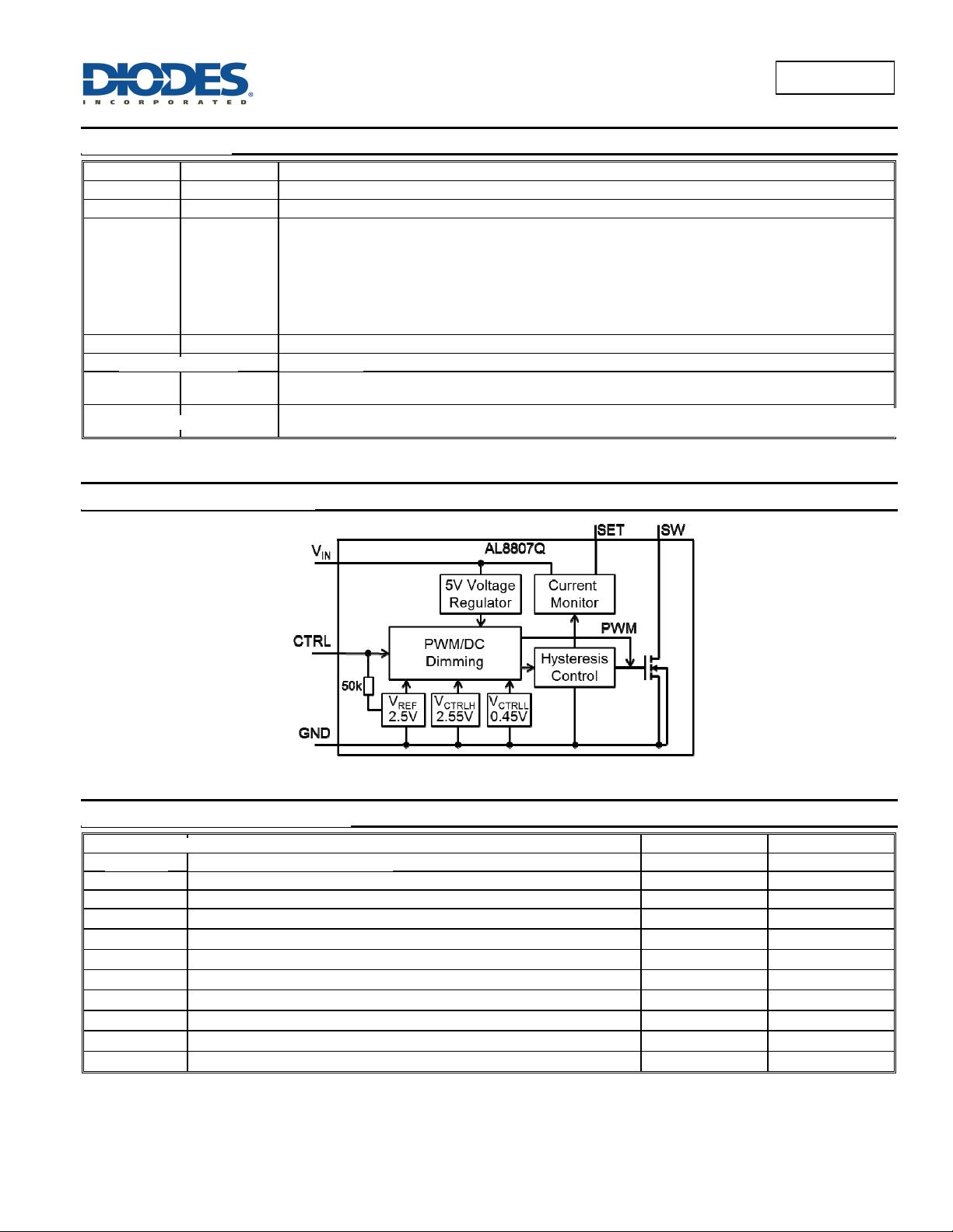
Maximum output current of AL8807Q is set via an external resistor
connected between the V
IN
and SET input pins. Dimming is achieved
by applying either a DC voltage or a PWM signal at the CTRL input
pin. An input voltage of 0.4V or lower at CTRL switches off the output
MOSFET simplifying PWM dimming.
The AL8807Q has been qualified to AEC-Q100 Grade 1 and is
Automotive Grade supporting PPAPs
Features
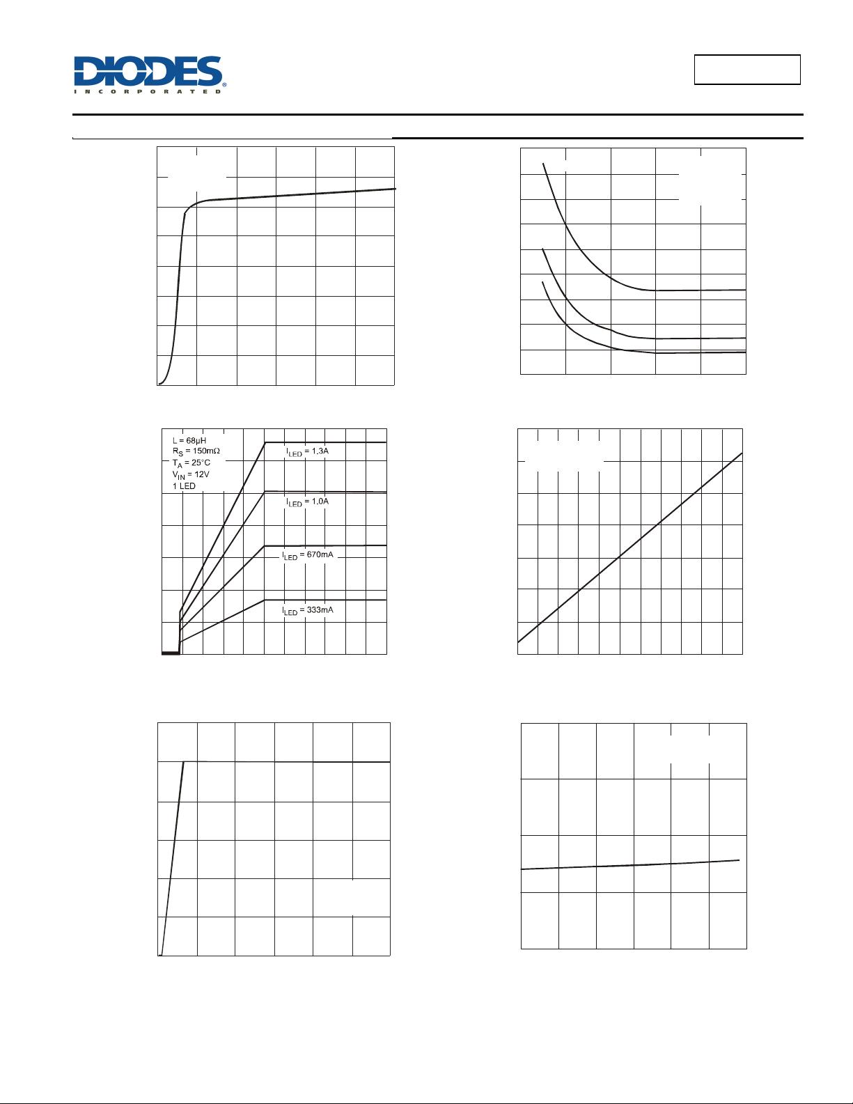
LED driving current up to 1.3A
Better than 5% accuracy
High efficiency up to 96%
Optimally controlled switching speeds
Operating input voltage from 6V to 30V
PWM/DC input for dimming control
Built-in output open-circuit protection
Automotive Grade with AEC-Q100 Qualification
MSOP-8EP: Available in “Green” Molding Compound (No Br, Sb)
Totally Lead-Free & Fully RoHS Compliant (Notes 1 & 2)
Halogen and Antimony Free. “Green” Device (Note 3)
Automotive Grade
Qualified to AEC-Q100 Standards for High Reliability
PPAP Capable (Note 4)
Pin Assignments
Applications
Automotive Interior LED Lamps
Automotive Exterior LED Lamps
Notes: 1. No purposely added lead. Fully EU Directive 2002/95/EC (RoHS) & 2011/65/EU (RoHS 2) compliant.
2. See http://www.diodes.com/quality/lead_free.html for more information about Diodes Incorporated’s definitions of Halogen- and Antimony-free, "Green"
and Lead-free.
3. Halogen- and Antimony-free "Green” products are defined as those which contain <900ppm bromine, <900ppm chlorine (<1500ppm total Br + Cl) and
<1000ppm antimony compounds.
4. Automotive products are AEC-Q100 qualified and are PPAP capable. Automotive, AEC-Q100 and standard products are electrically and thermally the same,
except where specified. For more information, please refer to http://www.diodes.com/quality/product_compliance_definitions/.
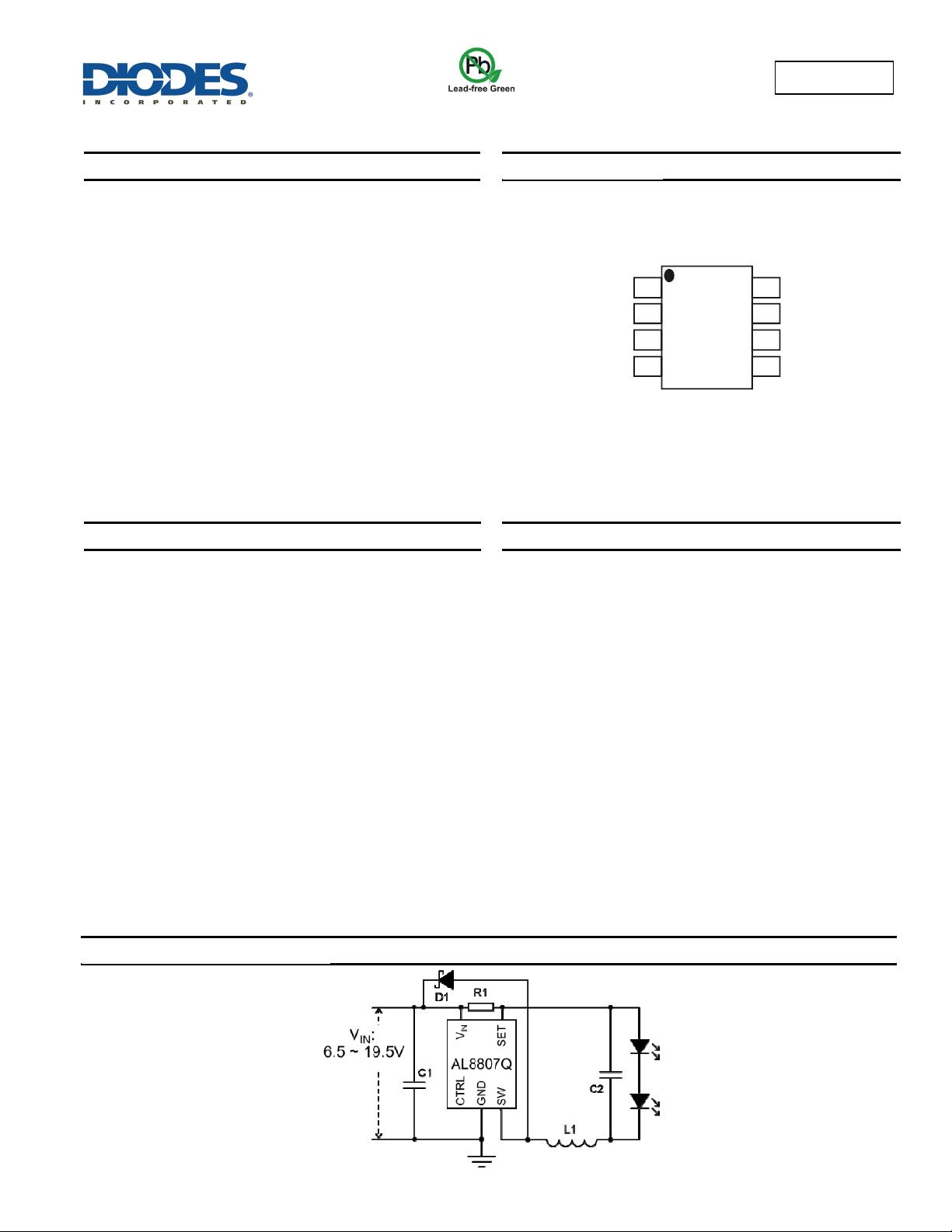
Typical Applications Circuit
(Top View)
MSOP-8EP
SET
GND
GND
CTRL
V
IN
N/C
SW
SW
文档编号:DS36904 Rev. 1 - 2
1 / 16
2014年3月
高效率低30v 1.3a
汽车级降压led驱动器
AL8807Q是一款降压DC/DC转换器,用于驱动具有恒流的led。该设备可以
驱动多达9个led,取决于led的正向电压,从6V到30V的电压源串联。串联的
LED提供相同的LED电流,导致均匀的亮度和消除镇流器电阻的需要。AL880
7Q开关频率高达1MHz,可控制上升和下降时间,以减少EMI。这允许使用
小尺寸的外部元件,从而最大限度地减少所需的PCB面积。
AL8807Q的最大输出电流通过连接在 V
IN
和set输入引脚之间的外部电阻设定
。调光通过在CTRL输入引脚处施加直流电压或PWM信号来实现。按CTRL键
时0.4V或更低的输入电压关闭输出MOSFET,简化PWM调光。
AL8807Q已通过AEC-Q100一级认证,是汽车级配套ppap
LED驱动电流高达1.3A
精度优于5%
效率高达96%
最佳控制切换速度
工作输入电压从6V到30V
PWM/DC输入调光控制
内置输出开路保护
通过AEC-Q100汽车等级认证
MSOP-8EP:可选“绿色”成型化合物(No Br, Sb)
完全无铅和完全符合RoHS标准(注1和2)
无卤素和锑。“环保”装置(注3)
符合AEC-Q100高可靠性标准
具备PPAP能力(注4)
销作业
汽车内饰LED灯
汽车外饰LED灯
1. 没有故意添加铅。完全符合欧盟指令2002/95/EC (RoHS)和2011/65/EU (RoHS 2)。
2. 有关Diodes Incorporated对无卤素和无锑的“绿色”定义的更多信息,请参阅http://www.diodes.com/quality/lead_free.html。
和无铅。
3.无卤素和无锑的“绿色”产品定义为含有<900ppm溴、<900ppm氯(<1500ppm总Br + Cl)和<1000ppm锑化合物的产品。4. 汽车产品通过AEC-Q100认证,具备PPAP能力。
汽车,AEC-Q100和标准产品在电和热方面是相同的,除非另有规定。欲了解更多信息,请访问http://www.diodes.com/quality/product_compliance_definitions/。
典型应用电路
(前视图)
设置
GND
GND
CTRL
西
北
偏
南
翻译仅供参考,如需更准确的信息,请参考英文版
AL8807Q
Document number: DS36904 Rev. 1 - 2
2 of 16
www.diodes.com
March 2014
© Diodes Incorporated
A
L8807Q
Pin Descriptions
Pin Name Pin Number Functions
SET 1 Set Nominal Output Current Pin. Configure the output current of the device.
GND 2, 3 GND Pin
CTRL 4
Dimming and On/Off Control Input.
Leave floating for normal operation.
(V
CTRL
= V
REF
= 2.5V giving nominal average output current I
OUTnom
= 0.1/R
S
)
Drive to voltage below 0.4V to turn off output current
Drive with DC voltage (0.5V < V
CTRL
< 2.5V) to adjust output current from 20% to 100% of I
OUTnom
A PWM signal (low level ≤ 0.4V and high level > 2.6; transition times less than 1us) allows the output
current to be adjusted below the level set by the resistor connected to SET input pin.
SW 5, 6 Switch Pin. Connect inductor/freewheeling diode here, minimizing track length at this pin to reduce EMI.
N/C 7 no connection
V
IN
8
Input Supply Pin. Must be locally decoupled to GND with >
2.2µF X7R ceramic capacitor – see applications
section for more information.
EP EP
Exposed pad/TAB connect to GND and thermal mass for enhanced thermal impedance. Should not be used as
electrical ground conduction path.
Functional Block Diagram
Absolute Maximum Ratings
(@T
A
= +25°C, unless otherwise specified.)
Symbol Parameter Ratings Unit
ESD HBM Human Body Model ESD Protection 4000 V
ESD MM Machine Model ESD Protection 300 V
ESD CDM Charged Device Model ESD Protection 1000 V
V
IN
Continuous V
IN
pin voltage relative to GND
-0.3 to +40 V
V
SW
SW voltage relative to GND -0.3 to +40 V
V
CTRL
CTRL pin input voltage -0.3 to +6 V
I
SW-RMS
DC or RMS Switch current 1.6 A
I
SW-PK
Peak Switch current (<10%) 2.5 A
T
J
Junction Temperature +150 °C
T
LEAD
Lead Temperature Soldering +300 °C
T
ST
Storage Temperature Range -65 to +150 °C
Caution: Stresses greater than the 'Absolute Maximum Ratings' specified above, may cause permanent damage to the device. These are stress ratings only;
functional operation of the device at these or any other conditions exceeding those indicated in this specification is not implied. Device reliability may be
affected by exposure to absolute maximum rating conditions for extended periods of time.
Semiconductor devices are ESD sensitive and may be damaged by exposure to ESD events. Suitable ESD precautions should be taken when handling
and transporting these devices.
文档编号:DS36904 Rev. 1 - 2
2 / 16
2014年3月
销的描述
销的名字 密码
设置标称输出电流引脚。配置设备的输出电流。
接地销
调光和开/关控制输入。
保持浮动状态以保证正常运行。
(V
CTRL
=V
REF
= 2.5V给出标称平均输出电流 I
OUTnom
=0.1/R
S
)
驱动到电压低于0.4V关闭输出电流
直流电压(0.5V < V
CTRL
< 2.5V)驱动,输出电流从 I
OUTnom
的20%调节到100%
PWM信号(低电平≤0.4V,高电平> 2.6;转换时间小于1us)允许将输出电流调整到低于连接到set输入引脚的电
阻设定的电平。
开关销。在这里连接电感/自由转动二极管,尽量减少这个引脚的轨道长度,以减少电磁干扰。
N / C 7 没有关系
输入电源引脚。必须与> 2.2µF X7R陶瓷电容器局部解耦到地-请参阅应用部分了解更多信息。
EP EP
暴露的pad/TAB连接到GND和热质量,以增强热阻抗。不宜用作接地电导通路。
功能框图
绝对最大收视率(@
除非另有说明,否则TA = +25°C。)
符号参数
ESD HBM 人体模型静电防护
ESD毫米 机器型号ESD保护
防静电清洁发展机制充电设备型号ESD保护
相对于地的连续 V
IN
引脚电压
-0.3到+40
相对GND的SW电压 -0.3到+40
CTRL引脚输入电压 -0.3到+6
DC或RMS开关电流
峰值开关电流(<10%)
结温
铅温焊
储存温度范围 -65到+150
大于上述“绝对最大额定值”的应力可能会对设备造成永久性损坏。这些只是压力评级;不暗示设备在这些或任何其他超出本规范中所指示的条件下的功能操作。长时
间暴露在绝对最大额定值条件下,可能会影响器件的可靠性。半导体器件是ESD敏感器件,暴露在ESD事件中可能会损坏器件。在搬运和运输这些设备时,应采取适
当的防静电措施。
AL8807Q
Document number: DS36904 Rev. 1 - 2
3 of 16
www.diodes.com
March 2014
© Diodes Incorporated
A
L8807Q
Recommended Operating Conditions (@T
A
= +25°C, unless otherwise specified.)
Symbol Parameter Min Max Unit
V
IN
Operating Input Voltage relative to GND 6.0 30 V
V
CTRLH
Voltage High for PWM dimming relative to GND 2.6 5.5 V
V
CTRLDC
Voltage range for 20% to 100% DC dimming relative to GND 0.5 2.5 V
V
CTRLL
Voltage Low for PWM dimming relative to GND 0 0.4 V
f
SW
Maximum switching frequency — 1 MHz
I
SW
Continuous switch current — 1.3 A
T
J
Junction Temperature Range -40 125 °C
Electrical Characteristics (@ V
IN
= 12V, T
A
= +25°C, unless otherwise specified.)
Symbol Parameter Conditions Min Typ Max Unit
V
INSU
Internal regulator start up threshold
V
IN
rising
— — 5.9 V
V
INSH
Internal regulator hysteresis threshold
V
IN
falling
100 — 300 mV
I
Q
Quiescent current Output not switching (Note 5) — — 350 µA
I
S
Input supply Current CTRL pin floating f = 250kHz — 1.8 5 mA
V
TH
Set current Threshold Voltage — 95 100 105 mV
V
TH-H
Set threshold hysteresis — — ±20 — mV
I
SET
SET pin input current
V
SET
= V
IN
-0.1
— 16 22 µA
R
CTRL
CTRL pin input resistance Referred to internal reference — 50 — kΩ
V
REF
Internal Reference Voltage — — 2.5 — V
R
DS(on)
On Resistance of SW MOSFET
I
SW
= 1A
— 0.25 0.4 Ω
t
R
SW rise time
V
SENSE
= 100±20mV, f
SW
= 250kHz
V
SW
= 0.1V~12V~0.1V C
L
= 15pF
— 12 — ns
t
F
SW fall time — 20 — ns
I
SW_Leakage
Switch leakage current
V
IN
=30V
— — 0.5 μA
JA
Thermal Resistance Junction-to-
Ambient (Note 6)
(Note 7) — 69 — C/W
JC
Thermal Resistance Junction-to-case
(Note 8)
(Note 7) — 4.3 — —
Notes: 5. AL8807Q does not have a low power standby mode but current consumption is reduced when output switch is inhibited: V
SENSE
= 0V. Parameter is
tested with V
CTRL
≤ 2.5V
6. Refer to figure 35 for the device derating curve.
7. Test condition for MSOP-8EP: Device mounted on FR-4 PCB (51mm x 51mm 2oz copper, minimum recommended pad layout on top layer and
thermal vias to bottom layer with maximum area ground plane. For better thermal performance, larger copper pad for heat-sink is needed
8. Dominant conduction path via exposed pad.
文档编号:DS36904 Rev. 1 - 2
3 / 16
2014年3月
推荐运行条件(@T
A = +25°C,除非另有说明。)
相对于地的输入电压
相对于GND, PWM调光的电压高
电压范围为20%至100%直流调光相对于地
相对于GND, PWM调光电压低
最大开关频率
连续开关电流
结温范围
电气特性(@ V
IN = 12V, TA = +25℃,除非另有说明。)
符号参数
内部调节器启动阈值
内部调节器迟滞阈值
静态电流 输出不切换(注5)
输入电源 CTRL引脚浮动f = 250kHz
设置电流阈值电压
设置阈值迟滞
SET引脚输入电流
CTRL引脚输入电阻 参考内部参考
内部基准电压
SW MOSFET的电阻研究
西南上升时间
V
SENSE
= 100±20mV, f
SW
= 250kHz
V
SW
= 0.1V~12V~0.1V C
L
= 15pF
西南降时
开关漏电流
热阻连接-环境(注6)
(注7)
热阻接线盒(注8)
(注7)
5. AL8807Q没有低功耗待机模式,但当输出开关被抑制时,电流消耗降低: V
SENSE
= 0V。参数测试用 V
CTRL
≤2.5V 6。设备降额曲线见图35。7. MSOP-8EP的测试
条件:器件安装在FR-4 PCB (51mm x 51mm 2oz铜)上,建议在顶层配置最小的焊盘布局,并在底层通过热通孔,最大面积地平面。为了获得更好的散热性能,
需要更大的铜衬垫作为散热片。主要的传导路径通过暴露的衬垫。
AL8807Q
Document number: DS36904 Rev. 1 - 2
4 of 16
www.diodes.com
March 2014
© Diodes Incorporated
A
L8807Q
Typical Performance Characteristics (@T
A
= +25°C, unless otherwise specified.)
0
50
100
150
200
250
300
350
400
0 5 10 15 20 25 30
V (V)
Supply Current (not switching) vs. Inpu t Current
IN
I (µA)
IN
V = 0V
V = V
T = 25C
CTRL
SE T IN
A
°
0
0.5
1
1.5
2
2.5
3
0 5 10 15 20 25 30
CTRL
A
V= Open
T = 25C
SE T IN
V = V
V (V)
V vs. In put Voltage
(CTRL pin o pen circuit)
IN
CTRL
V (V)
CTRL
900
800
200
0
F
R
E
Q
U
E
N
C
Y
(k
H
z)
700
100
600
300
400
01234
V
Figure 2. Switching Frequency vs. V
CTRL
CTRL
5
500
V = 12V
1 LED
R = 150m
T = 25°C
IN
SET
A
L = 33µH
L = 68µH
L = 100µH
100
90
70
60
40
30
20
0
LED
C
U
R
R
E
N
T
(A)
0.0 0.5 1.0 1.5 2.0 3.0 3.5 4.0 4.5 5.0 5.5
CTRL PIN VOLTAGE (V)
Figure 3. LED Current vs. V
CTRL
2.5
0.0 0.5 1.0 1.5 2.5 3.0 3.5 4.0 4.5 5.0
V (V)
Figure 4. I vs. V
CTRL
CTRL CTRL
2.0 5.0
80
60
-40
-60
I (µA)
CTRL
40
-20
0
20
V = V = 12V
T = 25°C
SET IN
A
-40 -15 10 35 60 85 110
AMBIENT TEMPERATURE (°C)
Figure 6. V VS. TEMPERATURE
CTRL
2.52
2.51
2.50
2.49
2.48
V (V)
CTRL
V = Open
V = V= 12V
CTRL
SET IN
文档编号:DS36904 Rev. 1 - 2
4 / 16
2014年3月
典型性能特征(@T
A = +25°C,除非另有说明。)
电源电流(不开关)vs.输入电流
V = V t =
25
CTRL
集
vs.输入电压
(CTRL引脚开路)
图2。开关频率vs. V
0.0 0.5 1.0 1.5 2.0 3.0 3.5 4.0 4.5 5.0 5.5
CTRL引脚电压(v)
图3。LED电流vs. V
CTRL
0.0 0.5 1.0 1.5 2.5 3.0 3.5 4.0 4.5 5.0
CTRL
CTRL
环境温度(℃)
CTRL
集
剩余15页未读,继续阅读
资源评论
沐风听雨_A
- 粉丝: 300
- 资源: 183
上传资源 快速赚钱
- 我的内容管理 展开
- 我的资源 快来上传第一个资源
- 我的收益 登录查看自己的收益
- 我的积分 登录查看自己的积分
- 我的C币 登录后查看C币余额
- 我的收藏
- 我的下载
- 下载帮助
安全验证
文档复制为VIP权益,开通VIP直接复制
信息提交成功