串行器-解串器_BU8255KVT-E2_规格书_ROHM(罗姆)串行器_解串器规格书.PDF
需积分: 5 116 浏览量
2023-11-26
15:13:50
上传
评论
收藏 1.03MB PDF 举报

LVDS Interface ICs
35bit LVDS Receiver
5:35 DeSerializer
BU8255KVT
●Description
LVDS Interface IC of ROHM "Serializer" "Deserializer" operate from 8MHz to 150MHz wide clock range, and
number of bits range is from 35 to 70. Data is transmitted seven times (7X) stream and reduce cable number
by 3(1/3) or less. The ROHM's LVDS has low swing mode to be able to expect further low EMI.
●Features
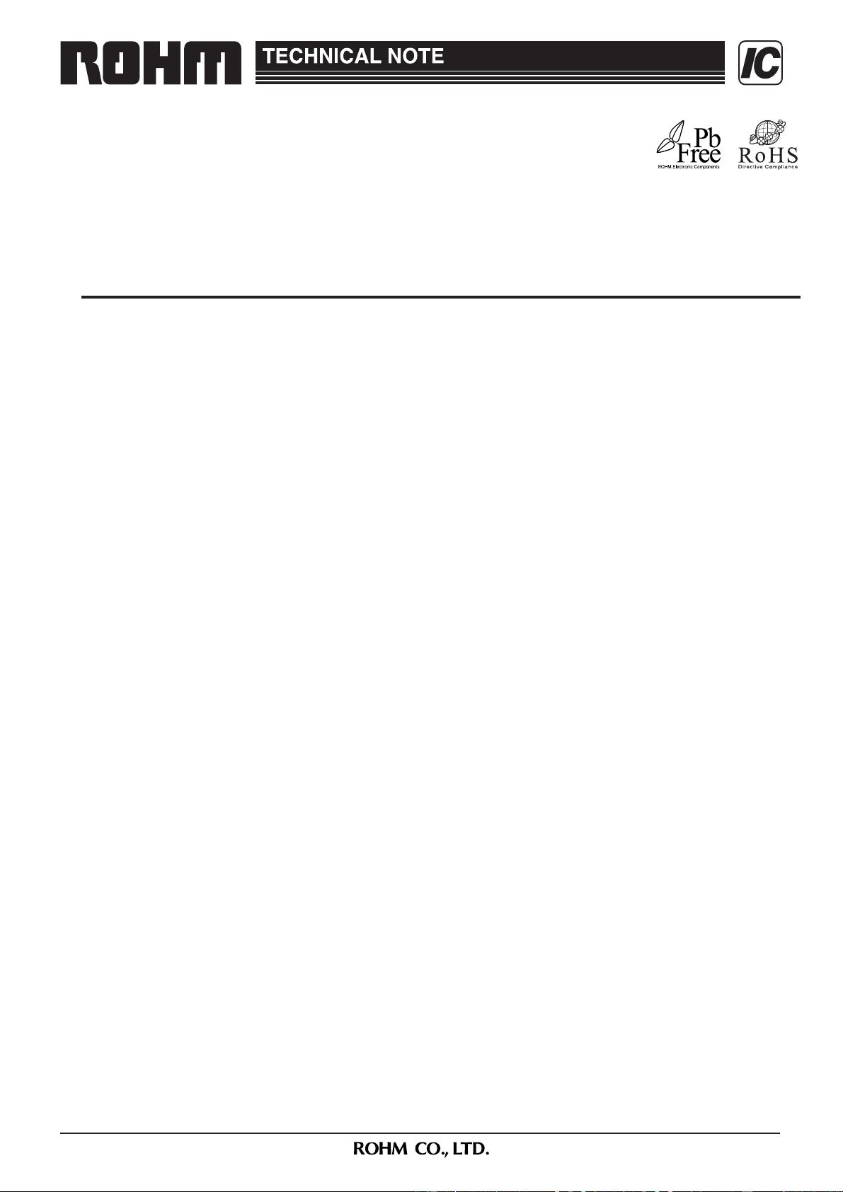
■Five channels of LVDS data stream are converted to 35bits data of parallel LVCMOS level outputs.
■30bits of RGB output data, 5bits of timing and control output data(HSYNC, VSYNC, DE, CTL1 and CTL2)
are transmitted available.
■Support clock frequency from 8MHz up to 112MHz.
■Support consumer video format including 480i, 480P, 720P and 1080i as well.
■Support many kinds of PC video formats such as VGA, SVGA, XGA and SXGA.
■Provide 784Mbps per 1ch or 3.92Gbps per device throughput rate using 112MHz clock rate.
■User programmable LVCMOS data output triggering timing by using either rising or falling edge of clock.
■30bit LVDS transmitter is recommended to use BU8254KVT.
●Applications
Flat Panel Display
◇Precaution
・This chip is not designed to protect from radioactivity.
・The chip is made strictly for the specific application or equipment.
Then it is necessary that the unit is measured as need.
・This document may be used as strategic technical data which subjects to COCOM regulations.
Status of this document
The Japanese version of this document is the formal specification.
A customer may use this translation version only for a reference to help reading the formal version.
If there are any differences in translation version of this document, formal version takes priority.
Jun.2008
LVDS接口ic
35位LVDS接收器5:35
反序列化器
ROHM“Serializer”“Deserializer”的LVDS接口IC工作在8MHz到150MHz的宽时钟范围内,位数范围为35到70。数据传输7
次(7X)流,减少电缆数3(1/3)或更少。罗姆的LVDS具有低摆幅模式,能够期望进一步降低EMI。
■5路LVDS数据流转换为35位并行LVCMOS电平输出数据。■可传输30位RGB输出数据,5位定时和控制输出数
据(HSYNC、VSYNC、DE、CTL1、CTL2)。■支持时钟频率从8MHz到112MHz。■支持消费视频格式,包括480i,
480P, 720P和1080i■支持VGA、SVGA、XGA、SXGA等多种PC视频格式。■使用112MHz时钟速率提供784Mbps
/ 1ch或3.92Gbps / 1ch设备吞吐率。■用户可编程LVCMOS数据输出触发定时使用时钟上升沿或下降沿。■30bi
t LVDS发射机推荐使用BU8254KVT。
●应用平板显示
这个芯片不是设计来防止辐射的。芯片是严格为特定的应用或设备制
造的。然后,有必要根据需要测量该单位。
本文件可作为战略技术数据使用,受COCOM法规约束。
本文件的状态
本文档的日文版本是正式的规范。
本翻译版本仅供客户参考,以帮助客户阅读正式版本。本文档的翻译版本如有差异,以正式版本为
准。
翻译仅供参考,如需更准确的信息,请参考英文版

剩余16页未读,继续阅读
资源评论


