没有合适的资源?快使用搜索试试~ 我知道了~
高速共阴极开关二极管,正向导通电压为0.7V。
资源推荐
资源详情
资源评论
DATA SHEET
Product specification
Supersedes data of 1997 Nov 24
1999 May 05
DISCRETE SEMICONDUCTORS
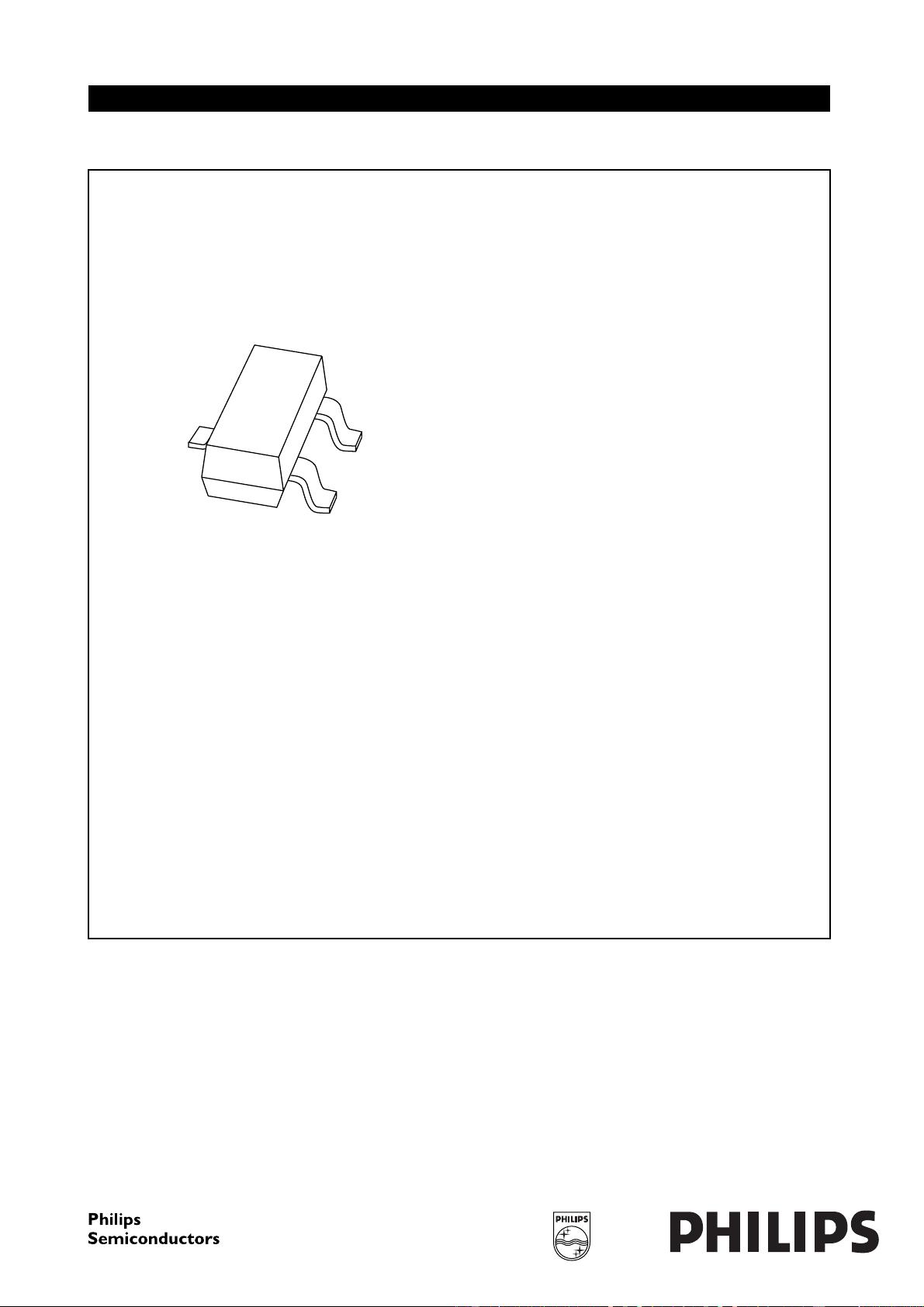
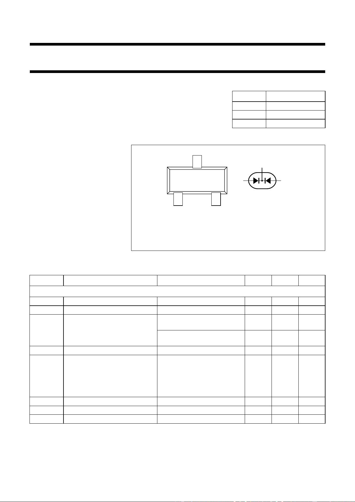
BAV70
High-speed double diode
b
ook, halfpage
M3D088
1999 May 05 2
Philips Semiconductors Product specification
High-speed double diode BAV70
FEATURES
• Small plastic SMD package
• High switching speed: max. 4 ns
• Continuous reverse voltage:
max. 70 V
• Repetitive peak reverse voltage:
max. 75 V
• Repetitive peak forward current:
max. 450 mA.
APPLICATIONS
• High-speed switching in thick and
thin-film circuits.
DESCRIPTION
The BAV70 consists of two
high-speed switching diodes with
common cathodes, fabricated in
planar technology, and encapsulated
in the small SOT23 plastic SMD
package.
PINNING
PIN DESCRIPTION
1 anode (a1)
2 anode (a2)
3 common cathode
Fig.1 Simplified outline (SOT23) and symbol.
Marking code: A4p = made in Hong Kong. A4t = made in Malaysia.
handbook, halfpage
21
3
Top view
MAM383
2
1
3
LIMITING VALUES
In accordance with the Absolute Maximum Rating System (IEC 134).
Note
1. Device mounted on an FR4 printed-circuit board.
SYMBOL PARAMETER CONDITIONS MIN. MAX. UNIT
Per diode
V
RRM
repetitive peak reverse voltage − 85 V
V
R
continuous reverse voltage − 75 V
I
F
continuous forward current single diode loaded; note 1;
see Fig.2
− 215 mA
double diode loaded; note 1;
see Fig.2
− 125 mA
I
FRM
repetitive peak forward current − 450 mA
I
FSM
non-repetitive peak forward current square wave; T
j
=25°C prior to
surge; see Fig.4
t=1µs − 4A
t=1ms − 1A
t=1s − 0.5 A
P
tot
total power dissipation T
amb
=25°C; note 1 − 250 mW
T
stg
storage temperature −65 +150 °C
T
j
junction temperature − 150 °C
1999 May 05 3
Philips Semiconductors Product specification
High-speed double diode BAV70
ELECTRICAL CHARACTERISTICS
T
j
=25°C unless otherwise specified.
THERMAL CHARACTERISTICS
Note
1. Device mounted on an FR4 printed-circuit board.
SYMBOL PARAMETER CONDITIONS MAX. UNIT
Per diode
V
F
forward voltage see Fig.3
I
F
= 1 mA 715 mV
I
F
= 10 mA 855 mV
I
F
=50mA 1 V
I
F
= 150 mA 1.25 V
I
R
reverse current see Fig.5
V
R
=25V 30 nA
V
R
=75V 2.5 µA
V
R
=25V; T
j
= 150 °C60 µA
V
R
=75V; T
j
= 150 °C 100 µA
C
d
diode capacitance f = 1 MHz; V
R
= 0; see Fig.6 1.5 pF
t
rr
reverse recovery time when switched from I
F
= 10 mA to
I
R
= 10 mA; R
L
= 100 Ω;
measured at I
R
= 1 mA; see Fig.7
4ns
V
fr
forward recovery voltage when switched from I
F
= 10 mA;
t
r
= 20 ns; see Fig.8
1.75 V
SYMBOL PARAMETER CONDITIONS VALUE UNIT
R
th j-tp
thermal resistance from junction to tie-point 360 K/W
R
th j-a
thermal resistance from junction to ambient note 1 500 K/W
剩余11页未读,继续阅读
资源评论
wanchy2008
- 粉丝: 0
- 资源: 3
上传资源 快速赚钱
- 我的内容管理 展开
- 我的资源 快来上传第一个资源
- 我的收益 登录查看自己的收益
- 我的积分 登录查看自己的积分
- 我的C币 登录后查看C币余额
- 我的收藏
- 我的下载
- 下载帮助
最新资源
- mysql-odbc-64-8.0.26
- 新建 Microsoft Word 文档 (2).docx
- 1652189183080063_42AD52629C553C7BC65694A425954A3F_1.apk
- 王都创世物语魔改版.apk
- Linear_regrassion_with_gradien_decent_example.ipynb
- 1719163625521533_1e90151d86c4cc2fadb97a0a82d0fc0e
- 虚拟现实课件-第五章 3物理建模
- 虚拟现实课件-第五章 2运动建模
- A1-ERP(资源协同)管理平台需求说明书.pdf
- 基于springboot+sureness的面向REST API资源无状态认证权限管理系统(源码+数据库+说明文档)
资源上传下载、课程学习等过程中有任何疑问或建议,欢迎提出宝贵意见哦~我们会及时处理!
点击此处反馈
安全验证
文档复制为VIP权益,开通VIP直接复制
信息提交成功