没有合适的资源?快使用搜索试试~ 我知道了~
serial spi flash mx25l4005 spec
资源推荐
资源详情
资源评论
REV. 1.1, SEP. 30, 2005
1
P/N: PM1236
MX25L4005
4M-BIT [x 1] CMOS SERIAL FLASH
FEATURES
GENERAL
• Serial Peripheral Interface (SPI) compatible -- Mode 0
and Mode 3
• 4,194,304 x 1 bit structure
• 128 Equal Sectors with 4K byte each
- Any Sector can be erased individually
• 8 Equal Blocks with 64K byte each
- Any Block can be erased individually
• Single Power Supply Operation
- 2.7 to 3.6 volt for read, erase, and program operations
• Latch-up protected to 100mA from -1V to Vcc +1V
• Low Vcc write inhibit is from 1.5V to 2.5V
PERFORMANCE
• High Performance
- Fast access time: 70MHz serial clock (15pF + 1TTL
Load) and 66MHz serial clock (30pF + 1TTL Load)
- Fast program time: 1.4ms(typ.) and 5ms(max.)/page
(256-byte per page)
- Fast erase time: 60ms(typ.) and 120ms(max.)/sector
(4K-byte per sector) ; 1s(typ.) and 2s(max.)/block (64K-
byte per block)
• Low Power Consumption
- Low active read current: 12mA(max.) at 70MHz,
8mA(max.) at 66MHz and 4mA(max.) at 33MHz
- Low active programming current: 15mA (max.)
- Low active erase current: 15mA (max.)
- Low standby current: 10uA (max.)
- Deep power-down mode 1uA (typical)
• Minimum 100,000 erase/program cycles
SOFTWARE FEATURES
• Input Data Format
- 1-byte Command code
• Block Lock protection
- The BP0~BP2 status bit defines the size of the area
to be software protected against Program and Erase
instructions.
• Auto Erase and Auto Program Algorithm
- Automatically erases and verifies data at selected
sector
- Automatically programs and verifies data at selected
page by an internal algorithm that automatically times
the program pulse widths (Any page to be programed
should have page in the erased state first)
• Status Register Feature
• Electronic Identification
- JEDEC 2-byte Device ID
- RES command, 1-byte Device ID
HARDWARE FEATURES
• SCLK Input
- Serial clock input
• SI Input
- Serial Data Input
• SO Output
- Serial Data Output
• WP# pin
- Hardware write protection
• HOLD# pin
- pause the chip without diselecting the chip
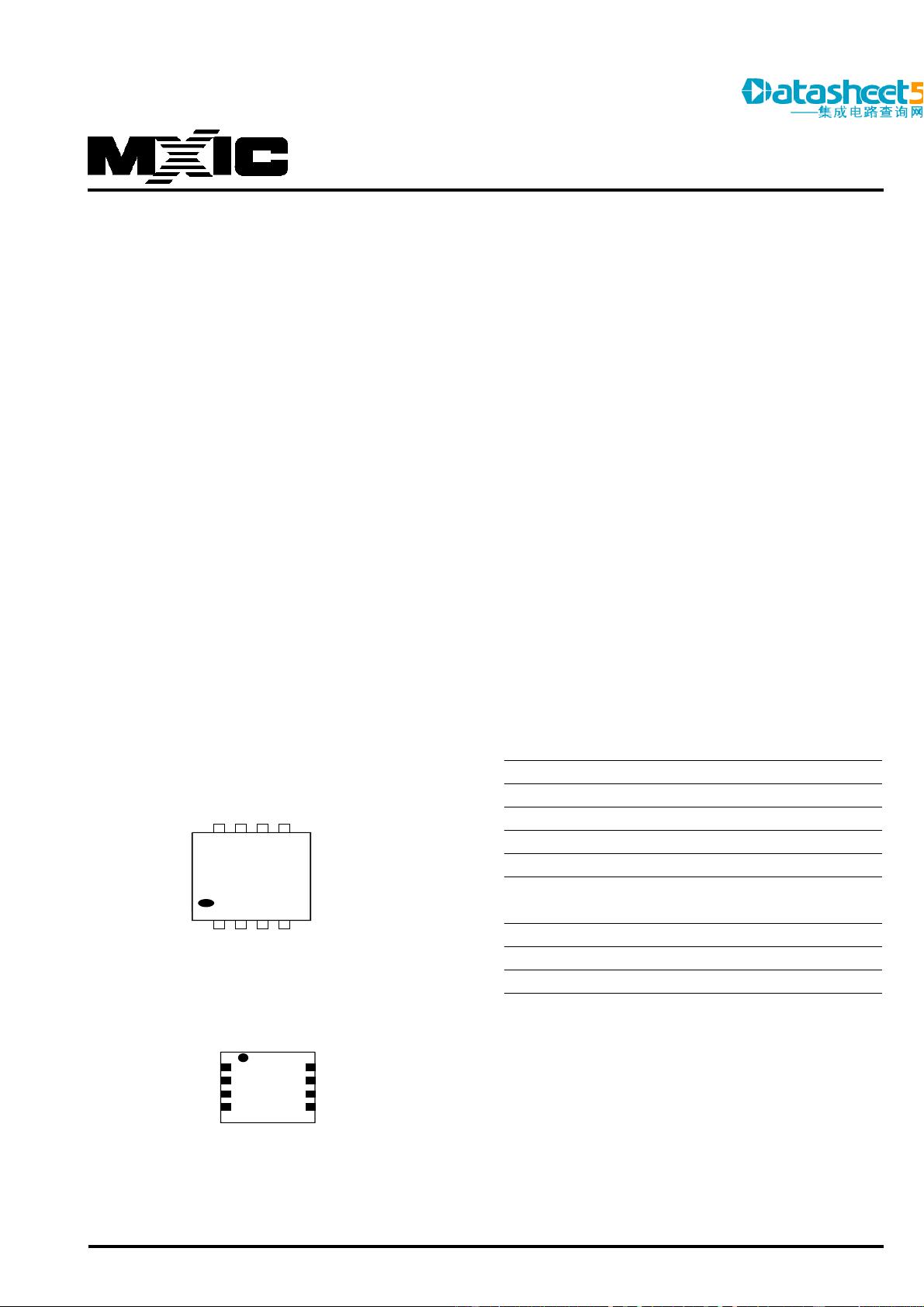
• PACKAGE
- 8-pin SOP (150mil)
- 8-pin SOP (200mil)
- 8-land SON (6x5mm)
- All Pb-free devices are RoHS Compliant
2
P/N: PM1236
REV. 1.1, SEP. 30, 2005
MX25L4005
PIN CONFIGURATIONS
SYMBOL DESCRIPTION
CS# Chip Select
SI Serial Data Input
SO Serial Data Output
SCLK Clock Input
HOLD# Hold, to pause the device without
deselecting the device
WP# Write Protection
VCC + 3.3V Power Supply
GND Ground
PIN DESCRIPTION
GENERAL DESCRIPTION
The MX25L4005 is a CMOS 4,194,304 bit serial Flash
memory, which is configured as 524,288 x 8 internally. The
MX25L4005 feature a serial peripheral interface and soft-
ware protocol allowing operation on a simple 3-wire bus.
The three bus signals are a clock input (SCLK), a serial
data input (SI), and a serial data output (SO). SPI access
to the device is enabled by CS# input.
The MX25L4005 provide sequential read operation on
whole chip.
After program/erase command is issued, auto program/
erase algorithms which program/ erase and verify the
specified page or byte /sector/block locations will be
executed. Program command is executed on page (256
bytes) basis, and erase command is executes on chip or
sector(4K-bytes) or block(64K-bytes).
To provide user with ease of interface, a status register is
included to indicate the status of the chip. The status read
command can be issued to detect completion status of a
program or erase operation via WIP bit.
When the device is not in operation and CS# is high, it is
put in standby mode and draws less than 10uA DC current.
The MX25L4005 utilize MXIC's proprietary memory cell,
which reliably stores memory contents even after 100,000
program and erase cycles.
8-PIN SOP (150/200mil)
8-LAND SON (6x5mm)
1
2
3
4
CS#
SO
WP#
GND
8
7
6
5
VCC
HOLD#
SCLK
SI
1
2
3
4
CS#
SO
WP#
GND
VCC
HOLD#
SCLK
SI
8
7
6
5
3
P/N: PM1236
REV. 1.1, SEP. 30, 2005
MX25L4005
BLOCK DIAGRAM
Address
Generator
Memory Array
Page Buffer
Y-Decoder
X-Decoder
Data
Register
SRAM
Buffer
SI
SCLK Clock Generator
State
Machine
Mode
Logic
Sense
Amplifier
HV
Generator
Output
Buffer
SO
CS#
4
P/N: PM1236
REV. 1.1, SEP. 30, 2005
MX25L4005
DATA PROTECTION
The MX25L4005 is designed to offer protection against
accidental erasure or programming caused by spurious
system level signals that may exist during power
transition. During power up the device automatically resets
the state machine in the Read mode. In addition, with its
control register architecture, alteration of the memory
contents only occurs after successful completion of
specific command sequences. The device also
incorporates several features to prevent inadvertent write
cycles resulting from VCC power-up and power-down
transition or system noise.
• Power-On Reset and an internal timer (tPUW) can
provide protection against inadvertant changes while
the power supply is outside the operating specification.
• Program, Erase and Write Status Register instructions
are checked that they consist of a number of clock
pulses that is a multiple of eight, before they are
accepted for execution.
• All instructions that modify data must be preceded by
a Write Enable (WREN) instruction to set the Write
Enable Latch (WEL) bit . This bit is returned to its reset
state by the following events:
- Power-up
- Write Disable (WRDI) instruction completion
- Write Status Register (WRSR) instruction completion
- Page Program (PP) instruction completion
- Sector Erase (SE) instruction completion
- Block Erase (BE) instruction completion
- Chip Erase (CE) instruction completion
• The Block Protect (BP2, BP1, BP0) bits allow part of
the memory to be configured as readonly. This is the
Software Protected Mode (SPM).
• The Write Protect (WP#) signal allows the Block
Protect (BP2, BP1, BP0) bits and Status Register
Write Disable (SRWD) bit to be protected. This is the
Hardware Protected Mode (HPM).
• In addition to the low power consumption feature, the
Deep Power-down mode offers extra software protec-
tion from inadvertent Write, Program and Erase in-
structions, as all instructions are ignored except one
particular instruction (the Release from Deep
Powerdown instruction).
• To avoid unexpected changes by system power supply
transition, the Power-On Reset and an internal timer
(tPUW) can protect the device.
• Before the Program, Erase, and Write Status Register
execution, instruction length will be checked on follow-
ing the clock pulse number to be multiple of eight base.
• Write Enable (WREN) instruction must set to Write
Enable Latch (WEL) bit before writing other instructions
to modify data. The WEL bit will return to reset state by
following situations:
- Power-up
- Write Disable (WRDI) instruction completion
- Write Status Register (WRSR) instruction completion
- Page Program (PP) instruction completion
- Sector Erase (SE) instruction completion
- Block Erase (BE) instruction completion
- Chip Erase (CE) instruction completion
• The Software Protected Mode (SPM) use (BP2, BP1,
BP0) bits to allow part of memory to be protected as
read only.
• The Hardware Protected Mode (HPM) use WP# to
protect the (BP2, BP1, BP0) bits and SRWD bit.
• Deep-Power Down Mode also protects the device by
ignoring all instructions except Release from Deep-
Power Down (RDP) instruction and RES instruction.
5
P/N: PM1236
REV. 1.1, SEP. 30, 2005
MX25L4005
Table 1. Protected Area Sizes
Status bit Protect level 4Mb
BP2 BP1 BP0
0 0 0 0 (none) None
0 0 1 1 (1 block) Block 7
0 1 0 2 (2 blocks) Block 6-7
0 1 1 3 (4 blocks) Block 4-7
1 0 0 4 (8 blocks) All
1 0 1 5 (All) All
1 1 0 6 (All) All
1 1 1 7 (All) All
剩余41页未读,继续阅读
资源评论
469751542
- 粉丝: 0
- 资源: 2
上传资源 快速赚钱
- 我的内容管理 展开
- 我的资源 快来上传第一个资源
- 我的收益 登录查看自己的收益
- 我的积分 登录查看自己的积分
- 我的C币 登录后查看C币余额
- 我的收藏
- 我的下载
- 下载帮助
安全验证
文档复制为VIP权益,开通VIP直接复制
信息提交成功