没有合适的资源?快使用搜索试试~ 我知道了~
dac7678 datasheet
需积分: 10 1 下载量 135 浏览量
2019-03-04
15:40:04
上传
评论
收藏 4.01MB PDF 举报
温馨提示
12-Bit, Octal-Channel, Ultra-Low Glitch, Voltage Output, Two-Wire Interface Digital-to-Analog Converter with 2.5V Internal Reference
资源推荐
资源详情
资源评论

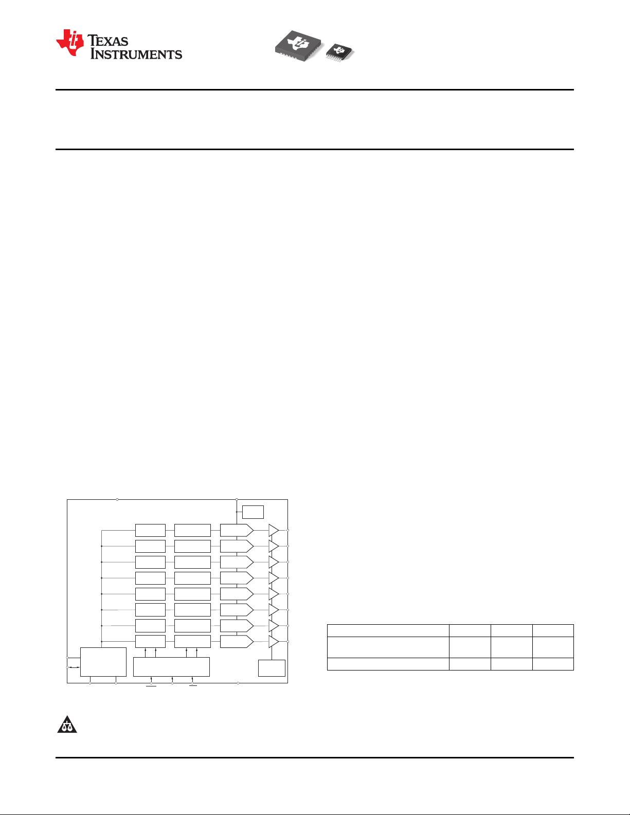
DAC7678
Data Buffer A
DAC Register A
Buffer Control Register Control
Control Logic
Input Control Logic
Power-Down
Control Logic
AV
DD
V
REFIN REFOUT
/V
12-Bit DAC
CLRLDACADDR0
SDA
SCL
2.5V
Reference
Data Buffer B
DAC Register B
Data Buffer C
Data Buffer D
Data Buffer E
Data Buffer F
Data Buffer G
DAC Register C
DAC Register D
DAC Register E
DAC Register F
DAC Register G
V H
OUT
Data Buffer H
DAC Register H
V G
OUT
V F
OUT
V E
OUT
V D
OUT
V C
OUT
V B
OUT
V A
OUT
GNDADDR1
12-Bit DAC
12-Bit DAC
12-Bit DAC
12-Bit DAC
12-Bit DAC
12-Bit DAC
12-Bit DAC
RSTSEL
DAC7678
www.ti.com
SBAS493C –FEBRUARY 2010–REVISED JANUARY 2014
12-Bit, Octal-Channel, Ultra-Low Glitch, Voltage Output, Two-Wire Interface
Digital-to-Analog Converter with 2.5V Internal Reference
Check for Samples: DAC7678
1
FEATURES
APPLICATIONS
23
• Relative Accuracy:
• Portable Instrumentation
– 1 LSB INL • Closed-Loop Servo-Control
• Glitch Energy: 0.15nV-s • Process Control
• Internal Reference: • Data Acquisition Systems
– 2.5V Reference Voltage (disabled by • Programmable Attenuation
default)
• PC Peripherals
– ±5mV Initial Accuracy (max)
DESCRIPTION
– 5ppm/°C Temperature Drift (typ)
The DAC7678 is a low-power, voltage-output, octal
– 25ppm/°C Temperature Drift (max)
channel, 12-bit digital-to-analog converter (DAC). The
– 20mA Sink/Source Capability
DAC7678 includes a 2.5V internal reference (disabled
• Power-On Reset to Zero Scale or Midscale
by default), giving a full-scale output voltage range of
5V. The internal reference has an initial accuracy of
– Devices in the TSSOP Package Reset to
±5mV and can source up to 20mA at the
Zero Scale
V
REFIN
/V
REFOUT
pin. The device is monotonic,
– Devices in the QFN Package Reset to Zero
provides very good linearity, and minimizes undesired
Scale or Midscale
code-to-code transient voltages (glitch).
• Ultra-Low Power Operation: 0.13mA/Channel
The DAC7678 uses a versatile, 2-wire serial interface
at 5V (without internal reference current)
that is I
2
C-compatible and operates at clock rates of
• Wide Power-Supply Range: +2.7V to +5.5V
up to 3.4MHz. Multiple devices can share the same
bus.
• 2-Wire Serial Interface ( I
2
C™ compatible)
• On-Chip Output Buffer Amplifier with Rail-to-
The DAC7678 incorporates a power-on-reset circuit
that ensures the DAC output powers up to either
Rail Operation
zero-scale or mid-scale until a valid code is written to
• Temperature Range: –40°C to +125°C
the device. These devices contain a power-down
feature, accessed over the serial interface that
reduces the current consumption of the device to
typically 0.42μA at 5V. Power consumption (including
internal reference) is typically 3.56mW at 3V,
reducing to 0.68μW in power-down mode. The low
power consumption, internal reference, and small
footprint make this device ideal for portable, battery-
operated equipment. The DAC7678 is drop-in and
functionally compatible with DAC5578, DAC6578,
and DAC7578. All devices are available in a 4x4
QFN-24 package and a TSSOP-16 package.
RELATED DEVICES 8-BIT 10-BIT 12-BIT
Pin- and Function-Compatible
— — DAC7678
(w/internal reference)
Pin- and Function-Compatible DAC5578 DAC6578 DAC7578
1
Please be aware that an important notice concerning availability, standard warranty, and use in critical applications of
Texas Instruments semiconductor products and disclaimers thereto appears at the end of this data sheet.
2I
2
C is a trademark of NXP Semiconductors.
3All other trademarks are the property of their respective owners.
PRODUCTION DATA information is current as of publication date.
Copyright © 2010–2014, Texas Instruments Incorporated
Products conform to specifications per the terms of the Texas
Instruments standard warranty. Production processing does not
necessarily include testing of all parameters.

DAC7678
SBAS493C –FEBRUARY 2010–REVISED JANUARY 2014
www.ti.com
This integrated circuit can be damaged by ESD. Texas Instruments recommends that all integrated circuits be handled with
appropriate precautions. Failure to observe proper handling and installation procedures can cause damage.
ESD damage can range from subtle performance degradation to complete device failure. Precision integrated circuits may be more
susceptible to damage because very small parametric changes could cause the device not to meet its published specifications.
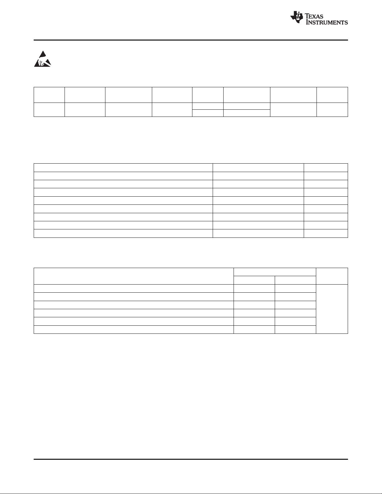
PACKAGE/ORDERING INFORMATION
(1)
MAXIMUM MAXIMUM MAXIMUM SPECIFIED
PACKAGE- PACKAGE PACKAGE
PRODUCT RELATIVE DIFFERENTIAL REFERENCE DRIFT TEMPERATURE
LEAD DESIGNATOR MARKING
ACCURACY (LSB) NONLINEARITY (LSB) (ppm/°C) RANGE
TSSOP-16 PW
DAC7678 ±1 ±0.25 25 –40°C to +125°C DAC7678
QFN-24 RGE
(1) For the most current package and ordering information see the Package Option Addendum at the end of this document, or see the TI
web site at www.ti.com.
ABSOLUTE MAXIMUM RATINGS
(1)
Over operating free-air temperature range, unless otherwise noted.
DAC7678 UNIT
AV
DD
to GND –0.3 to +6 V
Digital input voltage to GND –0.3 to +AV
DD
+ 0.3 V
V
OUT
to GND –0.3 to +AV
DD
+ 0.3 V
V
REFIN
/V
REFOUT
to GND –0.3 to +AV
DD
+ 0.3 V
Operating temperature range –40 to +125 °C
Storage temperature range –65 to +150 °C
Junction temperature range (T
J
max) +150 °C
Power dissipation (T
J
max – T
A
)/θ
JA
W
(1) Stresses above those listed under Absolute Maximum Ratings may cause permanent damage to the device. Exposure to absolute
maximum conditions for extended periods may affect device reliability.
THERMAL INFORMATION
DAC7678
THERMAL METRIC
(1)
UNITS
PW (16 PINS) RGE (24 PINS)
θ
JA
Junction-to-ambient thermal resistance 111.9 33.7
θ
JCtop
Junction-to-case (top) thermal resistance 33.3 16.9
θ
JB
Junction-to-board thermal resistance 52.4 7.4
°C/W
ψ
JT
Junction-to-top characterization parameter 2 0.5
ψ
JB
Junction-to-board characterization parameter 51.2 7.1
θ
JCbot
Junction-to-case (bottom) thermal resistance n/a 1.7
(1) For more information about traditional and new thermal metrics, see the IC Package Thermal Metrics application report, SPRA953.
2 Submit Documentation Feedback Copyright © 2010–2014, Texas Instruments Incorporated
Product Folder Links: DAC7678

DAC7678
www.ti.com
SBAS493C –FEBRUARY 2010–REVISED JANUARY 2014
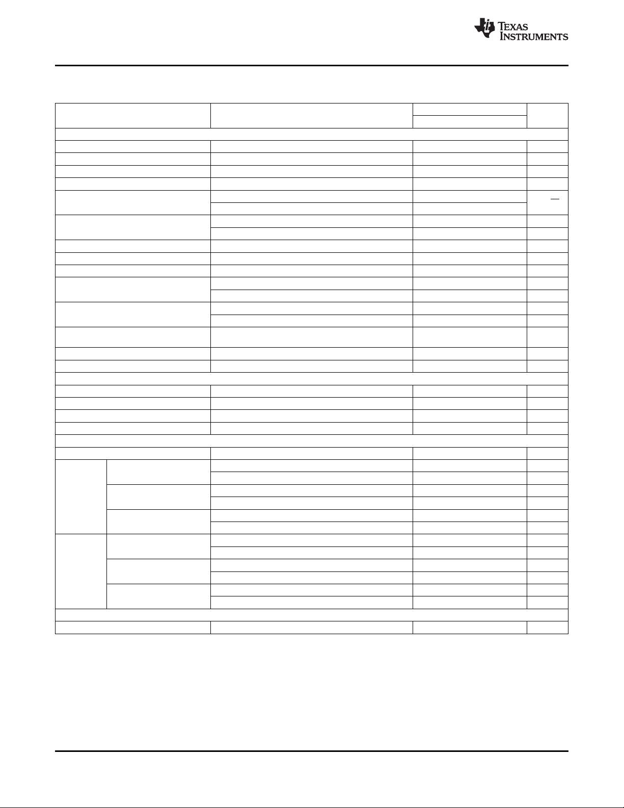
ELECTRICAL CHARACTERISTICS
At AV
DD
= 2.7V to 5.5V, External Reference Used, and over –40°C to +125°C, unless otherwise noted.
DAC7678
PARAMETER TEST CONDITIONS UNIT
MIN TYP MAX
STATIC PERFORMANCE
(1)
Resolution 12 Bits
Relative accuracy Measured by the line passing through codes 30 and 4050 ±0.3 ±1 LSB
Differential nonlinearity 12-bit monotonic ±0.1 ±0.25 LSB
Offset error Extrapolated from two-point line
(2)
, unloaded 0.5 ±4 mV
Offset error drift 3 μV/°C
Full-scale error DAC register loaded with all '1's ±0.03 ±0.2 % of FSR
Full-scale error drift 2 μV/°C
Zero-code error DAC register loaded with all '0's 1 4 mV
Zero-code error drift 2 μV/°C
Gain error Extrapolated from two-point line
(2)
, unloaded ±0.01 ±0.15 % of FSR
ppm of
Gain temperature coefficient ±1
FSR/°C
OUTPUT CHARACTERISTICS
(3)
Output voltage range 0 AV
DD
V
DACs unloaded, 1/4 scale to 3/4 scale 7 μs
Output voltage settling time
R
L
= 1MΩ, C
L
= 470 pF 12 μs
Slew rate 0.75 V/μs
R
L
= ∞ 470 pF
Capacitive load stability
R
L
= 2kΩ 1000 pF
Code change glitch impulse 1LSB change around major carry 0.15 nV-s
Digital feedthrough SCL toggling 1.5 nV-s
Power-on glitch R
L
= ∞ 3 mV
Channel-to-channel dc crosstalk Full-scale swing on adjacent channel 0.1 LSB
DC output impedance At midscale input 4.5 Ω
Short-circuit current DAC outputs shorted to GND 25 mA
Power-up time (including settling time) Coming out of power-down mode, AV
DD
= 5V 50 μs
AC PERFORMANCE
(3)
DAC output noise density T
A
= +25°C, at zero-code input, f
OUT
= 1kHz 20 nV/√Hz
T
A
= +25°C, at midscale input, 0.1Hz to 10Hz (external
DAC output noise 3 μV
PP
reference used)
(1) Linearity calculated using a reduced code range; output unloaded.
(2) 12-bit: 30 and 4050
(3) Specified by design or characterization; not production tested.
Copyright © 2010–2014, Texas Instruments Incorporated Submit Documentation Feedback 3
Product Folder Links: DAC7678

DAC7678
SBAS493C –FEBRUARY 2010–REVISED JANUARY 2014
www.ti.com
ELECTRICAL CHARACTERISTICS (continued)
At AV
DD
= 2.7V to 5.5V, External Reference Used, and over –40°C to +125°C, unless otherwise noted.
DAC7678
PARAMETER TEST CONDITIONS UNIT
MIN TYP MAX
INTERNAL REFERENCE
Output voltage T
A
= +25°C 2.495 2.5 2.505 V
Initial accuracy T
A
= +25°C –5 ±0.1 5 mV
Output voltage temperature drift
(4)
5 25 ppm/°C
Output voltage noise T
A
= +25°C, f = 0.1Hz to 10Hz 15 μV
PP
T
A
= +25°C, f = 1kHz, C
L
= 0μF 250
Output voltage noise density
nV/√Hz
(high-frequency noise)
T
A
= +25°C, f = 1MHz, C
L
= 0μF 50
Sourcing, T
A
= +25°C 500 μV/mA
Load regulation
(5)
Sinking, T
A
= +25°C 200 μV/mA
Output current load capability
(4)
±20 mA
Line regulation T
A
= +25°C 80 μV/V
Long-term stability/drift (aging)
(5)
T
A
= +25°C, time = 0 to 2160 hours 100 ppm
First cycle 200 ppm
Thermal hysteresis
(5)
Additional cycles 50 ppm
AV
DD
= 5.5V 420 μA
Internal reference current consumption
AV
DD
= 3.6V 400 μA
External V
REF
= 2.5V (when internal reference is disabled), all
External reference current 60 μA
eight channels active
V
REFIN
/V
REFOUT
pin reference input range 0 AV
DD
V
Reference input impedance Reference disabled 42 kΩ
LOGIC INPUTS
(4)
Input current ±1 μA
V
IN
L Logic input LOW voltage 2.7V ≤ AV
DD
≤ 5.5V GND–0.3 0.3×AV
DD
V
V
IN
H Logic input HIGH voltage 2.7V ≤ AV
DD
≤ 5.5V 0.7×AV
DD
AV
DD
+0.3 V
Pin capacitance 1.5 3 pF
POWER REQUIREMENTS
AV
DD
2.7 5.5 V
AV
DD
= 3.6V to 5.5V, V
IN
H = AV
DD
and V
IN
L = GND 1.02 1.4 mA
Normal mode, internal
reference switched off
AV
DD
= 2.7V to 3.6V, V
IN
H = AV
DD
and V
IN
L = GND 0.86 1.3 mA
AV
DD
= 3.6V to 5.5V, V
IN
H = AV
DD
and V
IN
L = GND 1.49 2.2 mA
Normal mode, internal
I
DD
(6)
reference switched on
AV
DD
= 2.7V to 3.6V, V
IN
H = AV
DD
and V
IN
L = GND 1.32 2 mA
AV
DD
= 3.6V to 5.5V, V
IN
H = AV
DD
and V
IN
L = GND 0.42 6 μA
All power-down modes
AV
DD
= 2.7V to 3.6V, V
IN
H = AV
DD
and V
IN
L = GND 0.25 4.7 μA
AV
DD
= 3.6V to 5.5V, V
IN
H = AV
DD
and V
IN
L = GND 3.67 7.7 mW
Normal mode, internal
reference switched off
AV
DD
= 2.7V to 3.6V, V
IN
H = AV
DD
and V
IN
L = GND 2.32 4.68 mW
AV
DD
= 3.6V to 5.5V, V
IN
H = AV
DD
and V
IN
L = GND 5.36 12.1 mW
Power Normal mode, internal
dissipation
(6)
reference switched on
AV
DD
= 2.7V to 3.6V, V
IN
H = AV
DD
and V
IN
L = GND 3.56 7.2 mW
AV
DD
= 3.6V to 5.5V, V
IN
H = AV
DD
and V
IN
L = GND 1.51 33 μW
All power-down modes
AV
DD
= 2.7V to 3.6V, V
IN
H = AV
DD
and V
IN
L = GND 0.68 16.92 μW
TEMPERATURE RANGE
Specified performance –40 +125 °C
(4) Specified by design or characterization; not production tested.
(5) Explained in more detail in the Application Information section of this data sheet.
(6) Input code = midscale, no load.
4 Submit Documentation Feedback Copyright © 2010–2014, Texas Instruments Incorporated
Product Folder Links: DAC7678

NC
AV
DD
V A
OUT
V C
OUT
V E
OUT
V G
OUT
NC
GND
V B
OUT
V D
OUT
V F
OUT
V H
OUT
1
2
3
4
5
6
18
17
16
15
14
13
DAC7678
7 8 9 10 11 12
24 23 22 21
20
19
NC
V /V
REFIN REFOUT
RSTSEL
ADDR1
ADDR0
CLR
NC
NC
LDAC
TWOC
SCL
SDA
(Thermal pad)
1
1
2
3
4
5
6
7
8
16
15
14
13
12
11
10
9
SCL
SDA
GND
V B
OUT
V D
OUT
V F
OUT
V H
OUT
CLR
LDAC
ADDR0
AV
DD
V A
OUT
V C
OUT
V E
OUT
V G
OUT
V /V
REFIN REFOUT
DAC7678
DAC7678
www.ti.com
SBAS493C –FEBRUARY 2010–REVISED JANUARY 2014
PIN CONFIGURATIONS
PW PACKAGE
RGE PACKAGE
TSSOP-16
QFN-24
(TOP VIEW)
(TOP VIEW)
(1) It is recommended to connect the thermal
pad to GND for better thermal dissipation.
PIN DESCRIPTIONS
16-PIN 24-PIN NAME DESCRIPTION
1 22 LDAC Load DACs.
2 11 ADDR0 Three-state address input 0
3 2 AV
DD
Power-supply input, 2.7V to 5.5V
4 3 V
OUT
A Analog output voltage from DAC A
5 4 V
OUT
C Analog output voltage from DAC C
6 5 V
OUT
E Analog output voltage from DAC E
7 6 V
OUT
G Analog output voltage from DAC G
V
REFIN
/
8 8 Positive reference input or reference output of 2.5V, if internal reference used.
V
REFOUT
9 12 CLR Asynchronous clear input
10 13 V
OUT
H Analog output voltage from DAC H
11 14 V
OUT
F Analog output voltage from DAC F
12 15 V
OUT
D Analog output voltage from DAC D
13 16 V
OUT
B Analog output voltage from DAC B
14 17 GND Ground reference point for all circuitry on the device
Serial data input. Data are clocked into or out of the input register. This pin is a bidirectional, open-
15 19 SDA
drain data line that should be connected to the supply voltage with an external pull-up resistor.
16 20 SCL Serial clock input. Data can be transferred at rates up to 3.4MHz. Schmitt-trigger logic input.
— 1 NC Not internally connected.
— 7 NC Not internally connected.
— 9 RSTSEL Reset select pin. RSTSEL high resets device to mid-scale; RSTSEL low resets device to zero-scale.
— 10 ADDR1 Three-state address input 1
— 18 NC Not internally connected.
Twos complement select. If the TWOC pin is pulled high, the DAC registers use twos complement
— 21 TWOC
format; if TWOC is pulled low, the DAC registers use straight binary format.
— 23 NC Not internally connected.
— 24 NC Not internally connected.
Copyright © 2010–2014, Texas Instruments Incorporated Submit Documentation Feedback 5
Product Folder Links: DAC7678
剩余55页未读,继续阅读
资源评论

风雪djq
- 粉丝: 1
- 资源: 6
上传资源 快速赚钱
 我的内容管理
展开
 我的资源
快来上传第一个资源
 我的收益 登录查看自己的收益
 我的积分
登录查看自己的积分
 我的C币
登录后查看C币余额
 我的收藏
我的收藏  我的下载
我的下载  下载帮助
下载帮助

 前往需求广场,查看用户热搜
最新资源
- 【IT教程网】17.第5章网络_远程过程调用.wmv
- 【IT教程网】16.第5章网络_网络客户端(二).wmv
- 【IT教程网】20.第6章数据(一).wmv
- arduino-esp32-core-installer
- 【IT教程网】19.第5章网络_Twisted.wmv
- 【IT教程网】15.第5章网络_网络客户端(一).wmv
- iServer服务批量配置工具
- 自动驾驶横纵向控制,纵向采用pid控制,横向采用mpc控制,根据的是车辆二自由度车辆动力学模型,得到各矩阵之后在S函数里面进行编写,纵向参考百度Apollo纵向双环PID控制算法,横向参考百度Apol
- 【IT教程网】24.第6章数据(五)_文件目录的模式匹配和包装rsync.wmv
- 【IT教程网】13.第4章文档与报告_信息格式化.wmv
- 【IT教程网】25.第6章数据(六)_元数据.wmv
- 【IT教程网】27.第8章操作系统什锦_Python中跨平台的UNIX编辑(一).wmv
- CCIE R&S路由与交换.pdf
- 【IT教程网】2.第2章IPython基础.wmv
- 【IT教程网】10.第3章文本_日志解析.wmv
- 【IT教程网】D09_01_包管理_easy_install.wmv
资源上传下载、课程学习等过程中有任何疑问或建议,欢迎提出宝贵意见哦~我们会及时处理!
点击此处反馈


安全验证
文档复制为VIP权益,开通VIP直接复制
 信息提交成功